As nanotechnology progresses, the photonics community is now tasked with measuring and identifying nanoscale materials with extremely small and varied structural parameters.
On the nanoscale, zero-dimensional (0D) structures are those that have truly nanoscale dimensions on the order of 10 nm in size or less, such as quantum dots.1 These 0D materials do not form a molecular network of multidimensionality, but remain as a nano-dimensional entity, with a size smaller than the de Broglie wavelength.
Nanomaterials such as nanowires or nanorods that form a molecular network and extend their length along one direction only while their diameter remains unchanged at <100 nm are termed one-dimensional (1D) nanomaterials. Alternatively, two-dimensional (2D) or planar nanomaterials like graphene and carbon nanotubes form a molecular network in both the x- and y-directions, with examples of 2D allotropes including borophene, germanene, silicene, phosphorene, and stanine. And finally, when aggregated in a size bigger than 100 nm, all materials fall in the realm of 3D, expanding their unit cells in all three orthogonal directions.While modern nanophotonic processes have facilitated the synthesis and production of these exotic nanomaterials, measurement and proper characterization of these nanoscale and subnanoscale materials pose new challenges to available instrumentation.
The TNS3DI terahertz time-domain imager from ARP (Harrisburg, PA) can analyze and quantify the above-mentioned materials, from 0D to 3D. In earlier research, the measurement of surface properties such as surface topography, texture, step height, and more—over a wide range of surfaces and materials—has been demonstrated.2 But the metrology of 0D–3D materials involves not only quantifying their size parameter and size distribution, it also involves quantifying the interaction of one nanomaterial with another.
Zero-dimensional quantum dots
A quantum dots (QD) is a nanocrystal that confines electrons and holes within its de Broglie wavelength; as such, these nanocrystals are only a few nanometers in size. At this scale, the electron is confined in a small region of space and occupies discrete energy levels that are analogous to those of a single atom. For this reason, QDs are also referred to as “artificial atoms.”
Quantum dots are most commonly fabricated using epitaxial techniques such as molecular beam epitaxy (MBE) or by colloidal chemistry. Ordinarily, an atomic force microscope (AFM) is used to image the QDs; a scanning electron microscope (SEM) can also be used when the QDs are deposited on a substrate such as a glass slide.
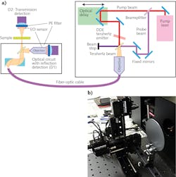
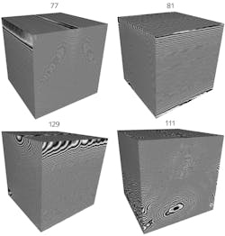
Alternatively, the ARP TNS3DI camera-less imaging technique characterizes 0D to 3D nanomaterials using terahertz radiation. The terahertz setup consists of a nanoscanner that digitizes an object over a 3D space (see Fig. 1).
It is well known that the resolution of images formed by a focusing lens on a recording medium—photographic film or a charge-coupled device (CCD)—is determined by the Abbe diffraction limit (ADL) that sets the resolution to the highest value of half the wavelength of the light used for imaging. Fortunately, ADL can be overcome (and higher-resolution images obtained) through terahertz multispectral reconstructive imaging.3
Since most materials are transparent to terahertz radiation, the ARP nanoscanner can probe and visualize subsurface features in a nondestructive, noncontact fashion. Together, hardware and software enable user-defined pixel sizes (voxel sizes in 3D), while a digital camera displays and records the processed signal from a sample with a fixed pixel size.
In a camera, an object is focused on a CCD or a focal plane array and a built-in processor displays the image on a screen and saves the image data in a file. In contrast, the terahertz technique eliminates the CCD and lens system by using a nanoscanner and a suitable computer algorithm for image generation and processing, eliminating the focusing lens and the CCD.
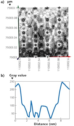
Here, the object to be imaged is scanned (digitized) along the three orthogonal axes for 3D imaging or digitized on a plane for surface imaging. A matrix containing the digitized reflected signal (or, equivalently, the transmitted signal) is recorded in a file and then processed by a suitable algorithm. Experimental measurement of the lattice constant of metallic nickel at 0.353 nm is the same value accepted in the scientific literature, therefore validating the terahertz imaging technique.One-dimensional structure characterization
Nanowires and carbon nanotubes are examples of 1D nanomaterials. Since their length is much bigger compared to their width (diameter), they qualify as 1D structures. Carbon nanotubes (CNTs) are cylindrical nanostructures that can be classified as single-walled and multi-walled carbon nanotubes (SWCNTs and MWCNTs).
With unique properties that lend themselves to extraordinary applications in electronics and optics, terahertz analysis with the TNS3DI can measure numerous properties. With a built-in terahertz time-domain spectrometer, it can perform both spectral analysis and deep-level spectroscopy, whereby spectra are collected at different depths of a sample as specified by the user.
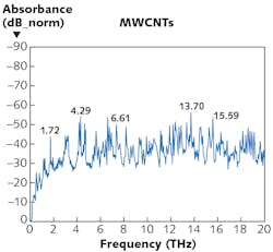
The TNS3DI implements a pump-probe technique with ARP’s proprietary terahertz source that works with a patented dendrimer dipole excitation (DDE) mechanism.4 Collecting the terahertz time-domain signal over a few picoseconds generates a signal known as an interferogram and the Fourier transform of that interferogram yields the absorption spectra of the sample (see Fig. 4). Prominent absorption peaks in the spectrum are observed at 1.72, 4.29, 6.61, 13.70, and 15.59 THz for the CNT samples. Here, data was collected between 0.1 and 30 THz—however, to increase legibility, the spectrum is only displayed up to 20 THz.Two-dimensional graphene
In theory, graphene is supposed to be a single layer of carbon atoms—a 2D nanomaterial. Graphene is mostly extracted from graphite—an allotrope of the element carbon meaning it possesses the same atoms, but they are arranged differently, giving the material different properties. In reality, however, graphene is an exfoliate possessing several layers of carbon sheets.
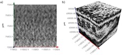
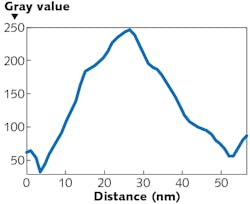
At ARP, terahertz multispectral computed imaging provides direct measurement of the graphene layers (that is, the number of sheets of graphene) in an exfoliate. It also measures the thickness of a single layer in the exfoliate. High-quality graphene is expected to have less than 10 layers in an exfoliate and should have a layer (sheet) thickness of <1 nm. Graphene oxide’s (GO) number of sheets in an exfoliate is higher and so is the thickness of each sheet.
Once the 3D image of a given exfoliate is generated, several useful parameters may be extracted. In addition to the number of layers and their thicknesses, a fast-Fourier transform (FFT) diffraction pattern can also be generated to describe crystallographic information. This volumetric imaging data not only allows layer-by-layer thickness measurement, but can also be used to obtain an FFT diffraction pattern.
Three-dimensional nanomaterials
A recently published paper by Rahman et al. in Novel Research in Sciences (NRS) investigated the dilation of nickel lattice from samples of alumina rods containing layers of metals and insulators that were subjected to what is known as a low-energy nuclear reaction (LENR) experiment.6 The samples were obtained from Brillouin Energy Corporation (Berkeley, CA), which demonstrated that the samples produced excess output energy compared to the input, under their experimental conditions.
However, Rahman et al. found a different explanation of this higher output energy than what was thought to be LENR process. The authors postulated that the higher-energy-generation effect observed in the experiment was most likely a “lattice-driven phenomenon” as opposed to the nuclear transmutation of LENR.
Rahman et al. conducted an in situ and ex situ systematic investigation that assumes a “time-crystal-like non-equilibrium” process is driving the energy balance. Time crystals—a newer concept—are states of matter whose patterns repeat at set intervals of time and space. They are systems in which time symmetry is spontaneously broken. A time crystal never reaches thermal equilibrium, as it is a type of nonequilibrium matter proposed in 2012.Using the terahertz time-domain technique, the authors analyzed a heated sample of crystalline nickel, which is more fluid-like than rigid near the glass-transition point (see Fig. 7). The applied thermal energy in a radio-frequency field sets the fluid-like nickel lattice into oscillation, producing a nonradiative transition that creates the increased heat energy. Instead of using an electron microscope, the terahertz technique breaks ground by using a larger terahertz wave that breaks the Abbe diffraction limit for lattice imaging. The experiment proves that the LENR is actually nonexistent and rather, a time-crystal-like non-equilibrium effect is driving the energy balance for what was considered to be a LENR phenomenon.
The ARP terahertz nanoscanner brings a new dawn of CCD-less imaging as nanomaterial characterization techniques have progressed from photographic film to CCD and finally to nanoscanner-based technologies. It is hoped this new technique will aid in solving a number of problems in industry and academia alike.
REFERENCES
1. A. Rahman et al., J. Biosens. Bioelectron., 7, 3, 1–8 (2016); doi:10.4172/2155-6210.1000221.
2. A. Rahman, “Application of TNS3DI as a Surface Metrology Tool,” doi:10.13140/rg.2.2.30786.73921 (2020).
3. A. Rahman and A. K. Rahman, IEEE Trans. Semicond. Manuf., 32, 1, 7–13 (Feb. 2019); doi:10.110 9/TSM.2018.2865167.
4. A. Rahman, A. K. Rahman, and D. A. Tomalia, Nanoscale Horiz., 2, 127–134 (Mar. 20, 2017); doi:10.1039/c7nh00010c.
5. W. Ghann et al., J. Nanomed. Nanotechnol., 10, 4, 535 (2019); doi:10.35248/2157-7439.19.10.535.
6. A. Rahman et al., Nov. Res. Sci. 2, 4, NRS.000545.2019 (2019); doi:10.31031/nrs.2019.2.000545.
