JOE O’KEEFFE and CARL JACKSON
A revolution in silicon (Si) photon-counting devices is currently under way, with a plethora of new detectors currently entering the market. These detectors enable a wide range of new applications from fluorescence-lifetime imaging to positron-emission tomography, radiation detection, high-energy physics, laser rangefinding (lidar), and particle sizing. There are even potential uses in emerging telecommunications applications such as quantum-key distribution for secure communications.
Historically, photon counters have been underpinned by three distinct technology platforms. The first of these, the photomultiplier tube (PMT), is based on the vacuum tube. These detectors have the advantage of a large photodetection area and are available in a variety of configurations. Furthermore, a large user base has made PMT detectors available at reasonable cost. But PMT detectors require operating voltages of more than 1000 V; their timing resolution is poor (around 500 ps); their quantum efficiency is limited by the photocathode to about 20%; and, most important, they are not compatible for implementation as high-density arrays or in miniaturized formats. The microchannel plate (MCP), a variant of the PMT, does have substantially better timing resolution (better than 100 ps), but suffers from a limited dynamic range (100 kHz/s). In addition, MCP detectors are very expensive and fragile.
The second photon-counting platform is based on the first-generation “reach-through” Si-detector structure. This structure requires a high voltage (higher than 100 V) and relies on a thick depletion region, which, while affording good responsivity at longer wavelengths (around 1000 nm), results in poor timing resolution. Also, reach-through structures are not compatible with standard Si-processing techniques and are not available in arrays, making them inherently unsuitable for imaging applications.
The third photon-counting-sensor technology platform is the electron-multiplied charge-coupled device (EMCCD), which is a variant on the standard CCD camera with a gain register incorporated into the output circuitry (see Laser Focus World, June 2005, p. 133). This is a multipixel imager (up to 1000 × 1000), but, because of its data-readout architecture, all timing resolution information is lost. The EMCCD also needs to be aggressively cooled (down to -100°C), making the device complicated and expensive.
Second-generation Si photon-counting devices
The newest, second-generation Si photon-counting technology will revolutionize low-light imaging. Based on the shallow-junction Geiger-mode biased Si diode, this technology has been developed and fine-tuned over several years to the point where it is now a mature processing technology. The performance advantages of the shallow junction include low timing jitter (less than 100 ps), low operating voltage (about 35 V), high count rate (10 M/s), high quantum efficiency (greater than 45%), and a wide spectral-sensitivity range (400 to 900 nm).1
The basic shallow-junction design includes an n+ into p junction that is close to the photon entry point at the top of the detector (see Fig. 1). The diode is fabricated in thin (5- to 15-µm) p-type substrates, which prevent deep generated carriers from slowing down detector response time.2 Dual top contacts allow flip-chip integration into novel detection platforms and point-of-use applications.3
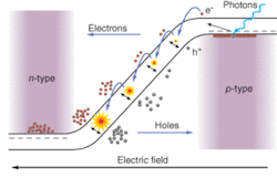
Photons entering into the junction generate electron-hole pairs, which separate and are amplified in the diode’s Geiger-mode biased junction (see Fig. 2). This results in a large, easily detectable (that is, low-noise) current pulse every time a photon enters the device. The high timing response that the device is capable of achieving allows precise photon-arrival time to be determined, which enables many of the advance techniques such as lidar and time-correlated single-photon counting to be performed.Single-photon-counting sensor
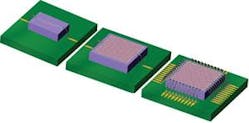
SensL, one company to commercialize these concepts, has evolved the technology into three product platforms (see Fig. 3).4 The first is a single high-timing-resolution sensor—a single-pixel photon-counting detector. Combined with the necessary current detection and quenching circuitry, this is a single-chip photon-counting device that is well suited to applications requiring an active area of 10 to 100 µm, high speed, and high timing resolution (see table).The ‘silicon photomultiplier’
Alternatively, multiple single-pixel photon-counting detectors can be fabricated in an array and all of the outputs connected to produce a large-area high-gain detector known as a silicon photomultiplier (SiPM). In this parallel configuration, each pixel has an integrated quench resistor and behaves as a photon-counting sensor, contributing a pulse of charge to the common output on detection of a photon. The device has an output proportional to the number of photons arriving at any particular time and is, in effect, a high-gain linear photodiode. It is an alternative to a linear avalanche photodiode (APD) or high-gain analog PMT.
The key differences between this new sensor design and traditional APD designs are a gain of many orders of magnitude higher (that is not sensitive to changes in temperature and biasing voltage), a faster response time, a larger active area, and bias voltage of only about 35 V. These devices can be tuned to detect photon fluxes ranging from single photons to millions of photons per second and are attracting great interest for nuclear medical imaging, low-power x-ray imaging, optical diffusion tomography imaging, nuclear particle detection, and high energy physics. The SiPM is a low-voltage, compact, robust, solid-state alternative to PMTs.
The photon-counting imager
Finally, the CMOS compatibility aspect of the shallow-junction technology enables arrays of diodes to be produced (see Fig. 3, right). In this arrangement, each diode or pixel is individually addressable using memory-architecture concepts. Combining this with integrated quenching circuitry produces a photon-counting imager. Several research groups working on such imagers have demonstrated the power of this technology. A device under development by SensL (called the DigitalAPD) has single-photon sensitivity yet retains photon-arrival timing information without requiring sensor cooling. This overcomes two of the major shortcomings of the EMCCD, which has been the historic low-light-imager technology of choice.
The applications of such novel imagers are varied and broad. A low-light imager that retains timing information will have many applications in fluorescence-lifetime measurement and medical imaging. A low-light imager that does not need extreme cooling, and hence has significantly lower power consumption, has many applications in fields such as portable security systems. A low-light imager with timing resolution can greatly benefit applications such as lidar, time-resolved fluorescence, and 3-D imaging. SensL is prototyping imagers that have a timing resolution of about 250 ps in arrays of sizes varying from 4 × 4 to 32 × 32 and eventually 1000 × 1000.
Challenges
There are a number of challenges yet to be overcome in the design and optimization of photon-imaging platforms based on shallow-junction technology. The voltage required to bias the device above breakdown is on the order of 35 V, which is higher than the normal CMOS operating voltages. This is a potential obstacle to combining the sensor and integrated electronics on the same Si die.
Three alternatives are being considered to solve this problem. The first is to use new high-voltage CMOS techniques that enable normal CMOS devices to operate together with these higher voltages. Alternatively, one can use SOI (silicon-on-insulator) wafers, which allow the separation of the diode from the electronics in two different Si layers and thus separate optimization.5 The third solution uses two separate Si wafers, one for the diodes or sensors and one for the pixel electronics. These are then flip-chipped or bonded together.
There is also a conflict to be resolved between the very shallow well depth required for high-speed CMOS and the relatively thick wells required for the detection of wavelengths longer than 700 nm.
While there are many challenges remaining to optimize this technology, the detectors that it enables will revolutionize low-light imaging. Many new and exciting applications will emerge such as in vivo point-of-use medical testing devices for real-time therapeutic diagnostics, low-cost high-performance night-vision technology, and laser-ranging imagers for environmental monitoring.
REFERENCES
1. D.M. Taylor et al., J. Modern Optics 51 (9-10) (June-July 2004).
2. J.C. Jackson et al., Appl. Phys. Lett. 80 (22) (June, 2002).
3. J. Kruger et al., J. Micromechanics and Microengineering 12 (July 2002).
4. J.C. Jackson et al., Proc. SPIE 2005, Semiconductor Photodetectors II, 5726-11 (January 2005).
5. A.M. Moloney et al., Electronics Lett. 39 (4) (February 2003).
Joe O’Keeffe is chief executive officer and Carl Jackson is chief technical officer of SensL, Lee House, Riverview Business Park, Bessboro Road, Cork, Ireland; e-mail: [email protected]; www.sensl.com.


