Two-dimensional arrays of electronic detectors are an attractive means for converting a visible image into digital data for subsequent computer editing and/or analysis. When compared to more-conventional photographic techniques, electronic imaging eliminates the time-consuming and messy process of chemical developing by directly generating a digital image file without an additional optical scanning step. On the downside, the spatial resolution of a typical charge-coupled-device (CCD) array is significantly less than that of conventional photographic film, and the cost of large arrays is high.
Well-established markets currently exist for electronic imaging technology in diverse applications that range from satellite imaging to portable "camcorder" systems. In astronomical observatories, large-area CCDs have replaced film as the technology of choice for recording the visual images produced by large telescopes and are routinely used in combination with fiberoptic visualization tools by the medical profession to "look" inside the human body. In the home-electronics market, camcorders with improved cost/performance features are introduced each year, while digital still cameras are rapidly gaining market acceptance. In the future, it is probable that digital cameras will replace conventional movie cameras, ushering in the age of the "electronic cinema."
Regardless of the array size or application in which it is used, a visible detector array operates by converting the light photons that strike the detector surface to electric charges that are stored within an array structure and subsequently read out by external circuitry. Different array types are distinguished by the specifics of charge storage and transmission. Individual detector elements within the array are referred to as "pixels," the size, number, and density of which are primary determinants of spatial resolution. In addition, array performance is dependent on the noise properties, dynamic range, spectral response, and sensitivity of the individual detector elements.
How CCDs work
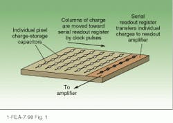
In a typical CCD array, photons that strike the individual pixel elements are converted into electrical charges that are stored in metal-insulator-semiconductor (MIS) capacitors. To first order, the amount of charge on a particular capacitor is proportional to the intensity of the light striking it, and the light-intensity distribution in the image is converted into a charge distribution in the detector. To read out the charge distribution, an array of electrodes spatially shifts the charge across the array surface to a readout register. In the simplest configuration, a line of pixels is shifted into a readout register that serially transfers the charge into an output amplifier that converts each pixel to an output pulse. Once the entire line has been read, the next one is shifted into the serial readout register and converted (see Fig. 1). This process is repeated until the charge distribution across the entire array has been converted to a string of voltage pulses that describe the light-intensity distribution across the array.Because a large number of charge transfers are required to completely read out a typical array, the carrier losses associated with a single pixel-to-pixel transfer must be small. While early designs failed miserably in this respect (charge-transfer efficiency [CTE] = 98%), due to their surface-channel design, newer, buried-channel devices can have CTE values as large as 99.999%. In most devices, CTE is reduced by carrier traps that are present in the bulk substrate, introduced during the array fabrication process, or induced by radiation. Process-induced traps are the most common source of low manufacturing yield, while radiation-induced traps are important for space-based applications.
Other basic parameters affecting array performance include the number of charges that can be stored in an individual pixel and the noise floor of the detector. The maximum number of charges that can be stored is determined by the MIS capacitor design and can exceed 100,000 electrons. The dynamic range of the detector is dependent on this parameter in addition to the maximum number of photons that can strike a pixel without producing "blooming" in the final image. Noise is generated by both the detection and amplification processes.
In addition to the dynamic range and noise of the individual detectors, the fidelity of a CCD image is influenced by overall array size, individual pixel size, spacing, and fill factor. Quantitatively, this performance is described by a wavelength-dependent modulation transfer function (MTF) that relates the two-dimensional (2-D) Fourier transform of the input image to that of the output. In addition to the obvious effects of pixel aperture and shape, the MTF of an array is affected by spatial carrier diffusion, temporal diffusion, and diffraction.
Alternative array designs
While the majority of 2-D array sensors are of the MIS/CCD design, alternative configurations can offer improved performance in specific applications. For example, charge-injection-device (CID) arrays have two storage capacitors for each pixel, one associated with a row bus and the other with a column bus. Readout is accomplished through the use of row/column decoders that allow random accessibility in the x-y plane with pixels being "reset" after the readout operation by charge injection.
Attractive characteristics of the CID configuration include a large-area fill factor, broadband operation with high quantum efficiency, and operation over a wide range of input intensities. On the negative side, low-noise operation is difficult to achieve.
The active-pixel-sensor (APS) design is a second alternative to the MIS/CCD approach in which the transistors needed for charge-to-voltage conversion are built into each pixel. Charge transport is unnecessary in these devices because readout occurs at the pixel level. When compared to CCD arrays, these devices have the advantage of a well-developed fabrication technology (CMOS) and potentially low cost. In addition, the random pixel addressability of APS devices can be desirable in certain applications.
On the downside, they are more prone to spatial nonuniformities in optical and electronic properties, and the increased complexity of each pixel establishes a lower size limit that is greater than that of CCD arrays. Because of their low cost and commercially compatible fabrication technology, APS sensors are expected to eventually replace CCDs in many nonscientific applications.
Single-chip color
Over the past several years, color video recording has developed as one of the most important applications for 2-D array technology. Starting with the development of relatively expensive and bulky devices, this technology has advanced to the point that a full-color camera with standard 8-mm resolution can be purchased for less than $400 and is only slightly larger than a grown man’s palm. These properties have made video-camera technology an important part of the consumer-electronics market. In the 1990s, video records of important personal events (weddings and birthdays, for example) replaced conventional photographs, and new video-based artworks are being displayed in major fine-art galleries throughout the world.
Technically, color video recording is differentiated from the monochrome process by the need to record three separate color-differentiated images. Although there are several different formats for transmitting color-television information (PAL, NTSC, and SECAM, for example) they all start with the separation of an image into blue, green, and red components. While this task can obviously be achieved by recording appropriately filtered images using three separate arrays, such systems tend to be large and costly. Cameras in which a full-color image is generated by a single detector array offer significant improvements in both parameters but have poorer spatial resolution.
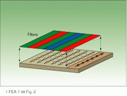
Single-chip color arrays typically use color filters that are aligned with individual columns of detector elements to generate a color video signal. In a typical stripe configuration, green filters are used on every other column with the intermediate columns alternatively selected for red or blue recording (see Fig. 2). To generate a color video signal using an array of this type, intensity information from the green columns is interpolated to produce green data at the red and blue locations. This information is then used to calculate a red-minus-green signal from red-filtered columns and a blue-minus-green signal from the blue ones. Complete red-minus-green and blue-minus-green images are subsequently interpolated from this data yielding three complete images. Commercial camcorders use a process similar to this to generate a color image but typically utilize more-complicated mosaic-filter designs.Single-chip cameras have the decided advantages of small size and reduced complexity, although the image quality is degraded with respect to a three-sensor system. Unfortunately, the use of alternate columns to yield color information decreases the spatial resolution in the final image. Assuming comparable array dimensions, cameras that use two or three sensors, generate a proportionally greater among of image data, thereby producing higher resolution images. Digital-signal-processing circuitry can be used to increase the fidelity of a single-chip image although multiple-chip cameras are typically used for applications requiring high-quality images.
Scientific and commercial applications
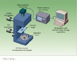
Given the increased power of dedicated microcomputer systems and the development of highly sophisticated image-processing software, the use of 2-D-array visible imaging systems is expected to increase at a rapid rate. At the present time, CCD imaging is the overwhelming choice for many scientific applications including astronomy, medical imaging, and remote sensing. For example, a large-area CCD array has been used in combination with an epi-illuminated fluorescence microscope to achieve a spatial resolution of 0.23 µm at an illumination wavelength of 450 nm (see Fig. 3). Utilizing technology that is nearly a decade old, this system could acquire an image with 1.4 million pixels every 3 to 10 seconds.Continued technical progress has led to larger arrays (2048 × 2048 pixels are common) and improved performance from hardware/software combinations that are designed for image acquisition and processing. Much of this progress is driven by the consumer-electronics market, and, in some cases, these products are appropriate for scientific use. For example, an imaging radar system under development at Sandia National Laboratories (Albuquerque, NM) produces fully rendered 3-D target images using a hardware/software combination that was originally developed for the video-game industry (see Laser Focus World, Sept. 1998, p. 91). According to the system`s developers, this system is well suited to the visualization of imaging radar data and is quite inexpensive.
Ongoing process
Perhaps the biggest push for the continued development of large, inexpensive CCD arrays comes from the entertainment industry, which ultimately wants to replace conventional movie film with high-resolution digital video systems. For such a system to ultimately be practical, CCD-based cameras with spatial resolutions matching those of conventional movie cameras must be developed along with high-brightness projectors suitable for use in the electronic cinema theaters of the future. The cost and performance requirements for such a system pose a significant technical challenge to the visual imaging industry but should ultimately lead to an entertainment environment in which high-resolution programming from a variety of sources can be displayed in a movie-theater format.
In the meantime, continued progress in the development of array-based imaging systems promises to significantly change the way in which we record and process visual images for a wide range of applications.
ACKNOWLEDGMENT
The author thanks the education department of SPIE for providing copies of notes from Terrence S. Lomheim`s courses "Use of CCDs and Solid State Sensors in Visible Imaging Applications" and "Color Imaging Using CCDs and Solid-State Sensors." Course dates and fees can be obtained from SPIE, POB 10, Bellingham, WA 98277-0010 or on the Web: www.spie.org.


