Nanoscribe

Eggenstein-Leopoldshafen 76344

COMPANY OVERVIEW

About Nanoscribe

Contact

Hermann-von-Helmholtz-Platz 6
Eggenstein-Leopoldshafen 76344
Germany
http://www.nanoscribe.com
49-721-981-9800
49-721-981-980130

More Info on Nanoscribe

Nanoscribe provides high-resolution 3D printers for microfabrication, photoresins and process solutions. The two-photon polymerization driven systems combine maskless lithography and additive manufacturing in one device. Applications: micro-optics, photonics, life-sciences, MEMS.

Products

Buyer's Guide

Photonic Professional GT2

3D printer for high-resolution microfabrication from nano- to macroscale

Articles

(Image credit: Vario-optics AG)
A photonic integrated circuit.
Optics

Advancing photonic integrated circuit packaging in Europe

European companies are now at the forefront of developing groundbreaking approaches to the packaging of photonic integrated circuits (PICs).
Nanoscribe
Laser Processing

Lithographic-based 3D printer achieves accuracy down to 100 nm

The Quantum X align lithographic-based 3D printer enables auto-aligned printing of freeform micro-optical elements directly onto optical fibers and photonic chips.
(Photo 100051973 / 3d © Keatanan Viya | Dreamstime.com)
Dreamstime M 100051973
Executive Forum

Cellink Life Sciences completes Nanoscribe acquisition

Nanoscribe specializes in 3D bioprinting based on two-photon polymerization technology.
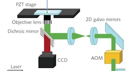
Optomechanical setup for writing a microlens on the tip of an endoscopic fiber via a two-photon process.
Optics

Aspherical microlens is laser-written onto the tip of a fiber-optic microendoscope

Using two-photon direct laser writing, a microscopic asphere is fabricated on the fiber tip of a fiber-optic microendoscope; the lens is aberration-free.
Nanoscribe
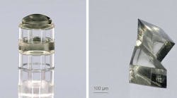
A compound lens system with two refractive elements is printed with Nanoscribe’s IP-n162 photoresin (left). The novel printing material has a high refractive index of 1.62, which expands the opportunities in creating new types of miniaturized optical systems. (The lens system was printed by Nanoscribe, with optical design by Simon Thiele, TTI GmbH TGU Printoptics.) A double Porro prism is 3D printed with Nanoscribe’s 3D microfabrication technology and the new high-refractive-index material IP-n162 (right).
Optics

New 3D-printing material for micro-optics has high refractive index

With both a high refractive index (1.62) and a low Abbe number (25), Nanoscribe’s new IP-n162 photoresin enables new types of micro-optical design.
Nanoscribe Handheld Oct
Optical Coherence Tomography

Photonic chip in development to enable mobile ophthalmic OCT

The novel photonic integrated technology is expected to bring optical coherence tomography (OCT) from stationary clinical use to broader, mobile use in ophthalmic care.
Nanoscribe
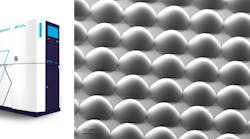
Microlens array (right) fabricated by Nanoscribe's Quantum X (left).
Optics

At LASER World of Photonics, Nanoscribe launches Quantum X for microoptics fabrication

The standalone enclosed machine, which fabricates refractive and diffractive micro-optics, was chosen as the most innovative product at the show.
Content Dam Lfw Print Articles 2019 02 1902lfw Nb F2
Research

3D-printed nanophotonic lens improves directivity of nanowire’s light emission

A nanophotonic lens with a complex structure, placed over a light-emitting nanowire, greatly reduces the divergence angle of the light output.
(Image: Nanoscribe)
Content Dam Lfw Online Articles 2019 01 Nanoscribe 3d Printed Lens
Optics

3D printed nanophotonic lens improves light directivity

Placed on an emitting nanowire tip, the lens uses nanoscale interference effects to achieve a high directivity.
(Image credit: Carl ZEISS)
Shown is the Nanoscribe subsidiary in the facilities of Carl ZEISS in Shanghai, China.
Lasers & Sources

Nanoscribe opens office in China to expand 3D nanoprinting business

Nanoscribe strives to strengthen its sales activities, reinforce existing business relationships, and further expand customer services.

Buyer's Guide Listing Information

Click here for listing information and directions on how to add or update your company.

Request More Information From Nanoscribe

By clicking above, I acknowledge and agree to Endeavor Business Media’s Terms of Service and to Endeavor Business Media's use of my contact information to communicate with me about offerings by Endeavor, its brands, affiliates and/or third-party partners, consistent with Endeavor's Privacy Policy. In addition, I understand that my personal information will be shared with any sponsor(s) of the resource, so they can contact me directly about their products or services. Please refer to the privacy policies of such sponsor(s) for more details on how your information will be used by them. You may unsubscribe at any time.

Additional content from Nanoscribe
(Image credit: Rachael Jayne and Alice White/Boston University)
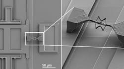
Shown is a 3D microstructure printed on a MEMS actuator.
Lasers & Sources

Nanoscribe prints 3D MEMS and microscopic components on integrated circuits

Nanoscribe 3D printers can print and integrate microscopic components directly on integrated circuits (ICs).
Content Dam Lfw Print Articles 2018 06 1806lfw Nb
Optics

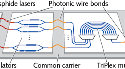
Free-space photonic wire bonds connect III-V and Si photonics on separate chips

Ultrafast-laser-written free-space photonic wire bonds connect III-V laser diodes on one chip with silicon photonics on another chip with an insertion loss of 0.4 dB.
(Image: ZEISS)
(From left to right): Martin Hermatschweiler, CEO of Nanoscribe, Prof. Dr. Thomas Hirth, vice president of KIT for Innovation and International Affairs at KIT, Prof. Dr. Michael Kaschke, president and CEO of ZEISS, Prof. Dr.-Ing. Holger Hanselka, president of KIT.
Lasers & Sources

Nanoscribe to move into the ZEISS Innovation Hub at KIT

Karlsruhe Institute of Technology's Hub will house other high-tech and digital start-ups and 'carve-outs' as well.
(Image: University of Stuttgart/ PI 4)
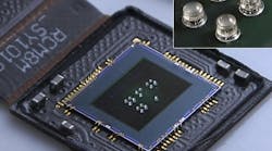
CMOS sensor with different focal lengths, four lenses each, for foveated imaging.
Optics

Nanoscribe’s optical 3D printers fabricate myriad types of micro-optics

Through two-photon polymerization, optics with high shape accuracy and optically smooth surfaces are created.
(Courtesy of Nanoscribe)
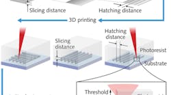
FIGURE 1. After an automated process of mesh fixing, slicing, and hatching, the desired structure is transferred into the photopolymer volume by scanning the laser's focus point in a layer-by-layer process. This 3D printing workflow is based on multiphoton absorption; polymerization is only triggered in the high-intensity region within the focal volume.
Lasers & Sources

Lasers for 3D Printing: Additive manufacturing with NIR lasers forms micro-sized parts

When common additive manufacturing (3D printing) technologies like stereolithography reach their limitations in resolution, 3D laser lithography achieves its full potential in...
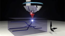
FIGURE 1. A conceptual image shows the laser-inscription process; nonlinear absorption occurs at the laser focus, resulting in white-light emission and highly localized energy deposition. A laser can effectively draw a waveguide in a bulk-glass material.
Lasers & Sources

Optical Manufacturing: Femtosecond-laser direct-written waveguides produce quantum circuits in glass

Integrated photonics can be written in glass via nonlinear absorption by focusing a short-pulse-duration laser into the glass; quantum-integrated-photonics (QIP) devices are being...
(Courtesy Nanoscribe)
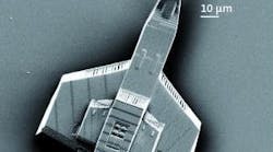
Three-dimensional (3D) laser printing on the micrometer and nanometer scale for a miniaturized spacecraft is reduced to less than one minute without loss of quality.
Research

Micro-nanostructure 3D printer from Nanoscribe uses new, fast laser lithography method

Eggenstein-Leopoldshafen, Germany--Nanoscribe, a spinoff of KIT, has developed what it calls the world's fastest 3D micro- and nanostructure printer.
(Images adapted from Science 317, p. 1749 (2007) by the Zhuang Research Lab at Harvard.)
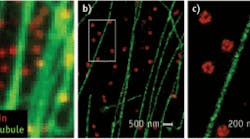
Conventional images of microtubules and clathrin-coated pits (CCPs) in a cell (a) lack the resolution provided by STORM (b and c). Microtubules (green) and clathrin (red) were stained with labeled antibodies.
Biophotonics Techniques

FLOW CYTOMETRY, MOLECULAR IMAGING: Cell Bio emphasizes easy access, low volume

Among the papers that the organizers of the Cell Bio show (the American Society for Cell Biology annual meeting, Dec. 13-17, 2008) chose to highlight for journalists covering ...