Micro- or nano-optics enable compact optical systems and pave the way to functionalities that cannot be achieved using more conventional types of optics. With the availability of ultraviolet (UV) imprint as a standard method for optics manufacturing, cost-efficient mass production of such optics is now a reality.
But when there is a need to integrate additional functionality—such as electrical traces, black apertures, etc.—into the optics module, in many cases, people fall back on complex and expensive processes like photolithography, which might not be ideal for the UV imprint process. Changing to a polymer-only process potentially saves costs, simplifies the process, and increases the reliability of the optical element.
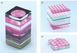
In simple terms, micro-optics are just a miniaturized version of conventional optics. One application where the advantages of reducing the size of optics is strikingly evident is in medical endoscopes. In recent years, using micro-optics and corresponding manufacturing techniques made it possible to shrink the full optics module, including the image sensor, to a cube with an edge length of <1 mm (see Fig. 1a).
Beyond reducing the dimensions of conventional optics, micro-optics also enable new and improved concepts for century-old optical tasks like projection systems. Instead of using one bulky setup for image projection, an array of microlenses can be used to parallelize the projection, achieving high light flux at a fraction of the size needed for conventional projection systems (see Fig. 1b).
When adjusting the dimensions from micro to nano, the light-steering method changes from refractive to diffractive and opens a plethora of possibilities. For example, diffractive optical elements (DOEs) can be used to change a collimated laser beam into virtually any desired light distribution. One notable example is generating a dot pattern for 3D sensing to detect the width, height, and depth of an object (see Fig. 1c).
Clearly, this new type of optics requires new methods for fabrication, because methods like injection molding are limited to their required feature sizes and precise alignment. UV micro/nanoimprint is now an established tool on standard machines, readily available from several manufacturers. In short, this process involves dispensing a liquid, transparent UV-curing material on a glass wafer, making contact with a stamp, defining the geometry of the optics (lenses, DOEs, etc.), curing by UV light, removing the stamp, and finally cutting into discrete modules (see Fig. 2).
Integrating functional layers: Apertures
Things get slightly more complicated if more features need to be integrated into an optical element. Apertures, for example, are key elements in many optical designs. Until now, one standard way to incorporate apertures into imprinted optics is to use the photolithographic process to create a structured chromium layer on a glass wafer and then imprint the optics onto the wafer.
On its own, this process is complex and expensive. It involves a multitude of steps: coating a glass wafer with a homogeneous chromium layer, depositing a photoresist, using a lithography step to structure the photoresist, chemically develop the photoresist, removing part of the chromium layer, and finally stripping the remaining photoresist.
This process also limits where such apertures can be applied, because the associated process works on glass wafers only and is typically not compatible with structuring a chromium layer on the polymer optics itself. Further issues might arise due to insufficient adhesion of the chromium layer on glass or of the polymer material on chromium. By directly embedding a functional (e.g., black) material into the polymer optics, many of these issues can be avoided.
One possibility of doing so is to imprint specifically defined channel structures together with the optical imprint, which can subsequently be filled by a black low-viscosity material that can be cured either by UV or temperature (see Fig. 3). Besides tremendously simplifying the process, another benefit of this option is that the thermomechanical properties of the optical transparent and the black material are much closer than those of chromium and polymer. This means that thermal stress due to CTE mismatch can be avoided and directly results in improved reliability, as proven in temperature cycling tests. Since glass substrates aren’t involved in this concept, the weight and height of the optics can effectively be minimized—which reduces cost.
Another possible approach is to start with a temporary carrier such as a plastic foil, onto which the apertures are manufactured by screen printing a light-blocking polymer. After UV or heat curing the polymer, a standard UV imprint follows on top, in which the optical structures can be precisely aligned to the apertures. After curing the transparent material and removal of the stamp, the carrier foil can be peeled off, resulting in a fully monolithic (all-polymeric) optical module containing integrated apertures (see Fig. 4).
Another advantage of either of these approaches is that the properties of the black materials can be tuned according to the optical design. If the design requires a high optical density in thinner layers, the material can be adjusted. If the optical designs require greater thickness or have less stringent requirements for optical density, then the material can be formulated accordingly. It is even possible to incorporate a spectral filter function directly in the polymer, for example, blocking of a certain wavelength range while transmitting in another wavelength range.
Integrating functional, electrically conductive layers
For some applications, integration of electrically conductive structures into the optical element is necessary. One example is the diffusor element used in time-of-flight or structured light sensors that form the collimated laser beam of the emitter. Conductive structures are used as safety net to detect potential damage of the diffusor element to avoid any threat from the collimated laser beam. A similar process to the one described for apertures can be used to manufacture such a safety net, with the only difference being instead of a black polymer, an isotropic electrically conductive adhesive (ICA) is used.
First, an ICA is screen printed onto a temporary carrier foil, containing various designs such as conductive traces or apertures. Then a transparent UV-curing material, such as DELO KATIOBOND OM614, imprints a nanograting onto that foil. Peeling off the carrier foil results in an all-polymer wafer with multiple nanostructured elements—each contain conductive structures directly manufactured within the transparent material. A resistance of 1.5 Ω, for example, shows the functionality of the structures.
Easy processes based on UV imprint technology are available to generate miniaturized optical elements like lenses or DOEs which contain additional functionalities like electric conductive paths or black apertures. Only two materials are needed to achieve this: one UV-curing transparent material to form the main optics and one UV or heat-curing filled material to provide the electrical conductivity or light-blocking property. Beyond the simplicity and cost-effectiveness of this process, this approach eliminates possible reliability issues such as thermal mismatching, because the two materials can be matched in their thermo-mechanical properties.


