3D interferometric microscopy reveals medical implant wear mechanisms

Oct. 10, 2011
Bruker Corp. says that 3D microscopy based on white-light interferometry can provide high-speed measurement with higher lateral resolution and better vertical measurement accuracy than competing technologies, including 2D stylus metrology and confocal microscopy.
Content Dam Lfw Online Articles 2011 10 1110lfwnbf1web

Bruker Corp. (Santa Barbara, CA) says that 3D microscopy based on white-light interferometry can provide high-speed measurement with higher lateral resolution and better vertical measurement accuracy than competing technologies, including 2D stylus metrology and confocal microscopy. Furthermore, 3D optical microscopy has a noncontact advantage: Stylus systems can induce mechanical filtering due to the contact-tip radius and can also damage the surface under test. In addition to surface-metrology and inspection applications in the automotive, aerospace, solar, and semiconductor markets, these systems are also suited to surface characterization of medical devices such as hip implants.

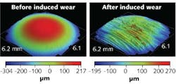
Using dual-LED illumination, a wavelength-filtering system that optimizes light levels for both smooth and rough surface textures, and an ultralow-noise CCD camera for subnanometer-resolution imaging, the ContourGT and NPFLEX 3D optical microscopes can examine the behavior of materials over a range of time scales as they are worn via cutting or grinding operations, or where material wear is produced due to constant contact with other components. These particular wear mechanisms are prominent in hip implants where there is contact by design. The system can also quantify material removal due to friction that can result in debris causing inflammation of the tissue surrounding the implant. The implants can be analyzed pre- and post-wear to automatically compute the volume-displacement and material-removal parameters, providing quantitative analysis of surface-wear scar depths and texture with a 5X better accuracy than gravimetric computations. Contact Matt Novak at [email protected].
About the Author

Gail Overton | Senior Editor (2004-2020)

Gail has more than 30 years of engineering, marketing, product management, and editorial experience in the photonics and optical communications industry. Before joining the staff at Laser Focus World in 2004, she held many product management and product marketing roles in the fiber-optics industry, most notably at Hughes (El Segundo, CA), GTE Labs (Waltham, MA), Corning (Corning, NY), Photon Kinetics (Beaverton, OR), and Newport Corporation (Irvine, CA). During her marketing career, Gail published articles in WDM Solutions and Sensors magazine and traveled internationally to conduct product and sales training. Gail received her BS degree in physics, with an emphasis in optics, from San Diego State University in San Diego, CA in May 1986.

Sponsored Recommendations

Request a free Micro 3D Printed sample part

April 11, 2024
The best way to understand the part quality we can achieve is by seeing it first-hand. Request a free 3D printed high-precision sample part.

How to Tune Servo Systems: The Basics

April 10, 2024
Learn how to tune a servo system using frequency-based tools to meet system specifications by watching our webinar!

Motion Scan and Data Collection Methods for Electro-Optic System Testing

April 10, 2024
Learn how different scanning patterns and approaches can be used in measuring an electro-optic sensor performance, by reading our whitepaper here!

How Precision Motion Systems are Shaping the Future of Semiconductor Manufacturing

March 28, 2024
This article highlights the pivotal role precision motion systems play in supporting the latest semiconductor manufacturing trends.

Voice your opinion!

To join the conversation, and become an exclusive member of Laser Focus World, create an account today!