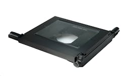
Microscope stage from Prior Scientific accommodates wafers up to 300 mm in diameter

Oct. 27, 2016
The H112 microscope stage offers a travel range >300 x 300 mm for precision scanning.

The H112 microscope stage offers a travel range >300 × 300 mm for precision scanning of semiconductor wafers, photomasks, flat-panel displays, and printed circuit boards. Using patented Intelligent Scanning Technology (IST), it accommodates wafers up to 300 mm diameter and samples up to 25 kg, and works with many robot arm wafer loaders.
Prior Scientific
Rockland, MA

www.prior.com

About the Author

LFW Staff

Published since 1965, Laser Focus World—a brand and magazine for engineers, researchers, scientists, and technical professionals—provides comprehensive global coverage of optoelectronic technologies, applications, and markets. With 80,000+ qualified print subscribers in print and over a half-million annual visitors to our online content, we are the go-to source to access decision makers and stay in-the-know.

Sponsored Recommendations

Request a quote: Micro 3D Printed Part or microArch micro-precision 3D printers

April 11, 2024
See the results for yourself! We'll print a benchmark part so that you can assess our quality. Just send us your file and we'll get to work.

Request a Micro 3D Printed Benchmark Part: Send us your file.

April 11, 2024
See the results for yourself! We'll print a benchmark part so that you can assess our quality. Just send us your file and we'll get to work.

Request a free Micro 3D Printed sample part

April 11, 2024
The best way to understand the part quality we can achieve is by seeing it first-hand. Request a free 3D printed high-precision sample part.

How to Tune Servo Systems: The Basics

April 10, 2024
Learn how to tune a servo system using frequency-based tools to meet system specifications by watching our webinar!

Voice your opinion!

To join the conversation, and become an exclusive member of Laser Focus World, create an account today!