Photodetectors capable of detecting a single photon are in increasing demand for applications such as quantum computing and imaging, time-of-flight LiDAR, and dark matter detection.
These applications have more stringent engineering requirements, such as high photon detection efficiency (nearly 100%), very low dark count rate, sensitivity in infrared, and instrument-limited time jitter. This is driving research and development into single-photon detectors, as well as the existing standard-bearer, a photomultiplier tube.
Single-photon detection and resolution
In response to a single photon, a photodetection system using a single-photon detector yields a signal-to-noise ratio (S/N) greater than 1. This means the incident photon has been detected to advance a count by 1 in a photon counting system or generate an analog current or voltage waveform distinguishable from the background electronic noise, which subsequently can be analyzed. Not every type of photodetector has this ability (a photodiode comes to mind), so an interesting question arises: What characteristics differentiate a photodetector that can detect a single photon from one that cannot?
All single-photon detectors have some form of positive feedback, where the absorption of an incident photon is followed by a cascading increase in the number of electrons making up the output signal. One photon results in more than one signal electron, and the photodetector has an intrinsic gain, μ, that equals that number of signal electrons. Positive feedback in a photodetector is a stochastic process—a repetitive absorption of a hypothetical identical photon would lead to some distribution of the gains, implying gain variation. Since gain variation affects the area under the curve of the output waveform, the system exhibits noise caused by the stochastic nature of the feedback. For a given feedback mechanism, we can derive a multiplicative and dimensionless excess noise factor, F, which represents the gain variation’s contribution to the detection noise. For a noiseless μ, F=1; otherwise, F > 1. In contrast, photodetectors unable to detect a single photon lack such positive feedback and produce one signal electron for the absorbed photon. For these detectors μ = 1 and F = 1.
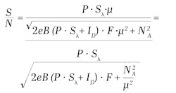
Suppose that monochromatic light with constant incident power, P, illuminates a photodetector, which is connected to a current-to-voltage converter such as a transimpedance amplifier. We can show that the detection S/N at the output of the amplifier is given by:
In this equation, Sλ is the photodetector’s spectral sensitivity and ID is its dark current. B is the detection bandwidth, NA is the amplifier noise (usually a function of the bandwidth), and e is the elementary charge. The equation shows that μ reduces the impact of NA on S/N. In the limit where μ→∞, S/N is limited by photon shot noise and/or dark current shot noise. In contrast, taking the limit μ→1, NA can become dominant at sufficiently low P, eventually making S/N <1. In summary, a large μ makes single-photon detection possible by effectively “suppressing” electronic noise. The equation also demonstrates that, all else being the same, increasing F worsens S/N. Furthermore, F affects the photodetector’s photon resolution.
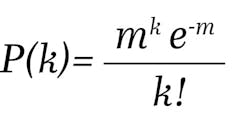
In the case of a single-photon detector whose output (the amplitude of the current pulse) is proportional to the number of incident photons, the detector should be illuminated repeatedly by monochromatic δ pulses, with an average number of photons per pulse equal to m. The actual number of photons in each δ pulse obeys Poisson statistics such that the probability of k photons in a pulse is:
A perfect detector with quantum efficiency QE = 1 and F = 1 coupled with a noiseless charge amplifier would generate a histogram of events with binned integrated charge on the horizontal axis (often referred to as channel) and normalized event frequency (number of events in a given bin divided by the total number of events) on the vertical axis.
The histogram would mimic the discrete Poisson probability distribution. Each column in the histogram corresponds to a specific integrated charge, and its height (normalized frequency) is equal to P(k) in the limit where the number of trials is infinite. The separation between channels depends on m and the characteristics of the amplifier. This ideal photodetector has photon number resolution because we can unambiguously determine the number of photons in every pulse. But if the detector has F > 1, the columns widen, even though the amplifier is still ideal and QE = 1. For sufficiently large F, the columns begin to overlap, and the detector, loses photon number resolution. The amplifier’s noise would further contribute to the widening of the columns, and QE < 1 would distort the histogram.
Optoelectronic characteristics
Every photodetector has a set of optoelectronic characteristics that describe its behavior in response to light, magnetic field, temperature change, or some other stimuli. Among dozens of characteristics, three are of principal importance: photon detection efficiency (η), dark count rate (nd), and single-photon time jitter (Δt).
Photon detection efficiency, η, is the probability that an incident photon triggers a measurable response. Most importantly and typically, η is a function of wavelength, being maximum at some given wavelength and declining to either side. The choice of material for the light-sensitive section of the detector is primarily responsible for its spectral response. For example, silicon-based detectors have their peak response in the visible, whereas those made of indium gallium arsenide (InGaAs) peak in the infrared. Other likely factors affecting η are construction architecture, biasing, and temperature.
Even in complete darkness, a detector outputs waveforms at the rate of nd, expressed in counts per second, or Hertz. These are called dark counts or, if time averaged, dark current, ID. Factors influencing nd are construction material and architecture, temperature, and biasing. Although both photon counting and analog measurements can be corrected for dark counts/current, the shot noise associated with dark events cannot be subtracted. With all else being the same, the higher nd or ID is, the lower the S/N. Device cooling and bias optimization are common methods of controlling and reducing nd or ID.
Repeated measurements of the response time can produce a Gaussian-like distribution. The full width at half maximum (FWHM) of this distribution is known as single-photon time jitter, Δt. Device architecture and construction, biasing, wavelength of light, and number of photons in a pulse affect Δt.
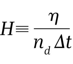
The above three characteristics can be combined to form a dimensionless figure of merit:
which is useful for comparing the performance of detectors belonging to the same family. In the case of an ideal detector η→1, nd→0, and Δt→0, making H→∞. The higher the H, the better the overall performance of the detector. However, caution is warranted in interpreting H as the denominator is the product of nd and Δt, so if one of these two characteristics is 0, H = ∞, regardless what the second characteristic is.
Single-photon detectors
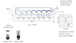
A photomultiplier tube (PMT) is a cold vacuum tube with three essential components: light-sensitive photocathode, a sequence of dynodes, and an anode. A schematic depiction of a PMT, biased with a resistive voltage divider, is shown in the top section of Figure 1 (see it at top of this page).
An incident photon is absorbed in the photocathode, and an electron is emitted into the vacuum of the PMT with the photoelectric effect. The electric field established inside the PMT accelerates the electron toward the first dynode. The energized electron collides with the first dynode, and through the process of secondary electron emission, δ1 electrons, on average, are emitted back into the vacuum. Subsequently, these are accelerated toward the second dynode; there, they collide, causing δ1 ∙ δ2 electrons to be re-emitted back into the vacuum. The sequence of acceleration, collision and electron secondary emission is repeated for every dynode, so that for N dynodes, the average number of electrons reaching the anode is approximately δ1 ∙ δ2 ∙∙∙ δN, typically 105–107, which is the PMT’s gain, μ.
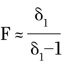
The large intrinsic gain μ of a PMT makes it a quintessential single-photon detector. But a typical PMT is not a photon-number-resolving device due to its gain noise, which is approximately given by:
and typically on the order of 1.3–1.4.
A single-photon avalanche photodiode (SPAD) is a p-n junction device that is reverse-biased beyond the breakdown voltage, known as the Geiger mode.
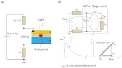
Figure 2a shows a SPAD in a circuit together with the quenching resistor, RQ, and the load resistor, RS. An absorbed photon produces an electron-hole (e-h) pair in the depletion region of the p-n junction. An internal electric field prevents the electron and hole from recombining and causes one of the charge carriers to drift into the avalanche region, where the electric field is sufficiently strong to energize the carrier to an energy at which its collision with the lattice atom leads to the atom’s ionization.The ionization produces another e-h pair; the starting point of the avalanche because the newly produced charge carriers can themselves impact-ionize additional lattice atoms, creating even more e-h pairs. When the avalanche starts, an increasing macroscopic current begins to flow in the circuit, causing the voltage on RQ to increase and the voltage on the SPAD to decrease. But when the voltage on the SPAD decreases and approaches the breakdown voltage, the internal electric field weakens to a point that it is no longer able to sustain the avalanche. Consequently, the avalanche eventually ceases, or is passively quenched. At the instant of quenching, the macroscopic current is at the maximum and then decreases in the recovery phase. During the avalanche and the recovery, the SPAD is insensitive to light (or its sensitivity is greatly reduced). Eventually the macroscopic current reaches 0; the voltage on the SPAD is fully restored and once again, the SPAD is in Geiger mode sensitive to light.
Figure 2b depicts a circuit with a SPAD represented by its model equivalent circuit (components within the red dashed rectangle). The switch closes at the onset of the avalanche and opens at the instant of quenching. The waveform, shown in blue, is the observed output current pulse from the SPAD. Its amplitude and area do not depend on the number of photons triggering the avalanche. This means that a single SPAD does not have a photon number resolution ability: we cannot measure the number of photons in a pulse with a SPAD.
A silicon photomultiplier (SiPM) is a pixelated device where each pixel (microcell) is a series combination of a SPAD and a quenching resistor, RQ. All the microcells are connected in parallel, resulting in a SiPM with two prongs: an anode and a cathode. The size of a microcell typically ranges from 10 × 10 µm2 to 100 × 100 μm2, and the size of the whole active area ranges from 1 × 1 mm2 to 6 × 6 mm2. The device is externally biased so voltage on each SPAD is above the breakdown voltage If a microcell absorbs a photon, the resulting charge carrier (an electron or hole, depending on the structure) can trigger an avalanche in the gain or avalanche region within the p-n structure, similar to a single SPAD.
The avalanche can produce 105–107 e-h pairs; this constitutes the gain, μ. The gain is linearly proportional to the product of the overvoltage and junction capacitance of the depletion region. Even though a SiPM is a pixelated device, it is not an image sensor, but rather an analog device whose output is a chronological superposition of current pulses from the firing microcells. One remarkable aspect of a SiPM is its very low excess noise (typically F ≈ 1.1, primarily due to optical crosstalk) permitting not only a single-photon detection but also photon number resolution.
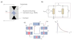
A superconducting nanowire single-photon detector (SNSPD) comes in a variety of architectures. In its most basic form, it is a meandering wire strip, typically less than 150 nm wide, less than 10 nm thick, but 10 s to 100 s μm long (see Fig. 3a). Examples of the materials for the wire are niobium nitride, tungsten silicide, or tantalum nitride. The wire operates in a superconducting state at a temperature dependent on the composition of the nanowire, ranging from less than 1 K to about 10 K.Figure 3b shows a biasing circuit with the SNSPD represented by its simplest model equivalent circuit (the components within the dashed red rectangle). In the whole circuit, Rs is the load resistor (typically 50 Ω) connected in parallel to the SNSPD. The resistance, Rn (t), is the normal-state (i.e., not superconducting) resistance of the SNSPD, which can reach a value as high as a few kΩ and is a function of time. The inductor, L, representing the kinetic inductance of the nanowire, is in series with a parallel combination of Rn (t). In the steady state, the switch is closed, making the resistance of the SNSPD equal 0. The current source, IBIAS, biases the circuit; the value of the current is set so that the current through the nanowire is below the critical value (above the critical current, the superconducting state is lost regardless of temperature) while in the superconducting state.
The circular graphics in Figure 3c describe the photodetection mechanics in an SNSPD. State (1) shows the nanowire in the superconducting state. The horizontal black arrows represent current distribution through the wire. State (2) depicts the photon absorption and formation of a hotspot (shown in red), characterized by locally suppressed superconductivity that has resistance greater than 0. State (3) shows that the current flows through the wire but outside of the hotspot, eventually increasing above the critical value. As a result, the resistive region grows, shown in State (4), and eventually creates a resistive barrier, as shown in State (5). The biasing current is being diverted to the load resistor, Rs, causing a rapidly increasing voltage on the resistor (see Fig. 3d). Heat dissipation into the thermal bath reduces resistivity of the barrier, demonstrated in State (6), ultimately bringing it to 0, shown in State (1). The switch closes in the model, and the SNSPD is once again fully in the superconducting state, ready for the next photon.
Although the SNSPD in the form described above does not have the ability to resolve photon numbers, it has a very low dark count rate (less than about 10 Hz) and small jitter (~30 ps). But other architectures exist using several SNSPDs, where the system does have the ability to resolve photon numbers.
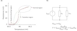
A transition edge sensor (TES) is a resistive microcalorimeter whose operation relies on a steep change of resistance with temperature as the material transitions from the superconducting state to the normal state (see Fig. 4a).Figure 4b shows the constant-voltage biasing circuit used to operate a TES. The device, represented by the resistor, RTES, (typically several Ωs) is in a parallel combination with the shunt resistor, RSH, such that RTES ≫ RSH. Located in a thermal bath, both resistors are in parallel with a biasing constant-current source, IBIAS. Because RTES ≫ RSH, a constant bias voltage exists across the TES. This form of biasing allows for a stable operation as opposed to a constant-current biasing, which can lead to unstable operation caused by runaway Joules heating. The inductor magnetically couples the current through TES to the readout circuitry consisting of a sequence of superconducting quantum interference devices (SQUIDs).
When TES absorbs an incident photon, the photon’s energy is converted to heat, which increases the device’s temperature. When the temperature changes, so does RTES and the current through it. The changing current is sensed by a SQUID via inductive coupling. Since TES is in a thermal bath, the heat eventually dissipates, bringing TES back to its steady state. A TES has a photon number resolving ability, provided the change of its resistance stays within the transition region; if the change brings it to the normal region, the TES’s response becomes saturated.
Although a TES has one of the largest time jitter among the single-photon detectors, it does have two distinguishing advantages: one of the highest photon detection efficiency at the important 1500 nm wavelength and negligible dark count rate (which, if it exists, is due to stray photons and cosmic rays).The table provides some basic characteristics of the detectors described above. The middle three columns give a typical photon detection probability at λ=1,550 nm, dark count rate, and single-photon jitter, respectively.
REFERENCE
1. C. M. Natarajan, M. G. Tanner, and R. H. Hadfield, Supercond. Sci. Technol., 25, 063001 (2012).
