Detection of optical radiation is required in many applications, from the discovery of new subatomic particles to the detection of brain activation by a motor task such as finger tapping. The sensitivity of these measurements depends on the signal-to-noise ratio of the optical detector and the signal-processing electronics that boost the signal to a level high enough to be detected with an analog-to-digital converter. The signal size is determined by the efficiency of the quantum-mechanical conversion of the photon to an electron times the gain of the signal-processing electronics. In selecting a detector, we tend to focus only on the efficiency of the optical-to-electrical conversion, losing sight of the fact that even the best electronics will introduce noise as they multiply the signal.
Methods of amplification
If the signal is large enough, very little or no gain is needed and the signal-to-noise ratio is said to be shot-noise limited. In this case, the only noise is the statistical noise that is a consequence of the transformation from photons to electron, which is given by N = (2qI)1/2, where q is the charge of an electron and I is the photocurrent generated by the detector. This is the ideal signal-to-noise ratio. Most phenomena do not produce enough light to allow detection of the photocurrent directly, so the trick is to multiply the signal without adding too much noise—a task usually done by preamplifiers and amplifiers.
But two types of detectors have intrinsic gain: the photomultiplier (PMT) and the avalanche photodiode (APD). For very low light levels, the PMT is the detector of choice. The APD works quite well, however, for light levels in the near-infrared, at which most PMTs have poor conversion efficiencies, or at moderate light level. Unlike the PMT, the APD is relatively insensitive to magnetic fields, making it the detector of choice for use in high-magnetic-field environments.
In an APD, light is absorbed in the depletion layer, generating an electron-hole pair (see Fig. 1). The internal electric field drives the holes toward the p+ side, while the electrons are driven to the n+ side. The drift speed of the electrons and holes is dependent on the size of the electric field, with the heavier holes moving more slowly than the electrons. As the electric field increases, the carriers (electrons and holes) collide with the crystal lattice. If the field is increased, the collision results in ionization of the lattice into an electron-hole pair. This new carrier pair will also collide with the lattice, producing an avalanche multiplication.The holes and the electrons have different efficiencies of ionization. The ideal APD would have zero efficiency for ionization by holes. As the voltage across the APD is increased, the multiplication also increases, until the device breaks down and acts like a short circuit instead of a detector. Most APDs operate at gains well below the breakdown region, usually at a gain of between 50 and 500.
Compensating for temperature dependence
The gain of an APD at a given electric field depends on the temperature. As the temperature increases, the lattice vibrations of the semiconductor also increase, resulting in more collisions between the electrons and the lattice. This effect actually produces a drop in gain because the collisions take place before the electrons can be accelerated by the internal electric field to an energy that is sufficient for ionization. This temperature dependence requires that the APD be thermally stabilized or that the bias voltage be constantly adjusted to compensate for temperature changes—both methods have been used. The former minimizes the dark current, because the device is usually cooled below room temperature.
When no voltage is applied to an APD, the spectral response is similar to that of a photodiode. Red light penetrates deeper into the structure, passing through the avalanche region, while some of the blue light is absorbed in the avalanche region. Thus, the gain of an APD is wavelength dependent. By modifying the APD structure, it is possible to enhance the blue-light gain.
In the absence of light, a dark current flows in the APD. Some of this current is surface leakage current (Ids), which does not pass through the avalanche region and is not multiplied. Another portion of the dark current (Idg) passes through the gain region. Often, people think the dark current itself affects the measurement. Unless the dark current is saturating the signal-processing system, however, only the shot noise from the dark current is a problem.
The major source of noise for an APD operating at low light levels results from the avalanche process. This is because the ionization process is not uniform, but is instead a statistical process. The noise current of an APD is given by:
In = (2q(IL + Idg)BM2F + 2qIdsB)1/2
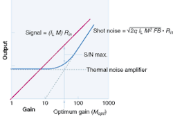
where IL is the photocurrent generated by the photon-to-electron conversion; it is what would be produced if the APD were a simple photodiode. In addition, B is the bandwidth of the system, M the gain, and F the excess-noise factor. If the gain process were noise-free, then F would be 1; manufacturers work very hard to minimize F. While ideally F could be as low as 2, it is typically between 2.5 and 5, depending both on the gain and the wavelength. As the gain increases, the excess noise factor increases by a fractional power of between 0.2 and 0.5. Signal to noise is a function of input light (see Fig. 2).Counting single photons
An APD can also be used in the so-called Geiger mode. The device is operated at a voltage above breakdown. When a photoelectron is generated, it produces a self-sustaining avalanche with an output gain of 106. The current pulse must be actively or passively quenched. This quenching process limits an APD to detecting less than a few million photons per second. Such APDs are well suited for single-photon counting. Unfortunately, they have very small active areas of between 100 and 300 µm.
The small active area of the single-photon-counting APDs limits them to very low-light-level applications in which it is possible to image the light onto a very small spot. For example, they have been used as detectors in fluorescent confocal microscopes. Some researchers like these devices because the 100-µm active area acts both as the pinhole and the detector. Others find alignment with such a small active area a problem. Some gene sequencers utilize near-infrared dyes to detect DNA. The dyes are used because there is no interference with the intrinsic fluorescence from the sample. The DNA is separated by capillary electrophoresis. The capillary is only between 25 and 100 µm in diameter, so it is relatively easy to collect the light and image it into a 100-µm-diameter spot. Aligning the image with the detector is the challenge. One other application of indium gallium arsenide (InGaAs) photon-counting APDs is the secure transmission of cryptography keys using single photons (see www.idquantique.com for an example).
Analog APDs do not have as much gain as the photon-counting type, but are used in many more applications because of their larger areas, which can exceed 10 mm in size. Often they are used for applications that have previously used photodiodes, but require increased sensitivity. A typical smoke detector, for example, will use a light-emitting diode and a photodiode. Particulate matter is detected by measuring the light scattered by the particulate matter. The gain of the APD increases the signal-to-noise ratio at low light levels, making it possible to detect lower particulate concentrations and hence detect a fire sooner. This is very important in factories or refineries. Avalanche photodiodes have also been used for monitoring other particles such as dust or bacteria.
Other APD applications
Many different approaches have been suggested for connecting the "last mile" between the phone company's office and the customer. One method that has been proposed is using free-space optical communications. This approach has the advantage that the infrastructure costs are relatively low since no streets need to be excavated. In addition, no FCC or other government approval is required. To keep the laser power as low as possible, it is necessary to use an APD with as large an area as possible. The data transmission speed of the optical link will dictate the size of the APD. Both silicon and InGaAs APDs have been used for this application.
Retinal scanning can detect defects that could cause blindness such as a detached retina or changes in the optic nerve resulting from glaucoma. Two mirrors are used to scan a combined green and red laser beam over the retina. Two separate APDs with filters are used to detect the reflected light. The red beam probes structures below the surface into the choroid region, while the green light probes only the epithelium layer. The gain of the APD permits making measurements at laser light levels that will not damage the retina.
At CERN (Conseil Europeen pour la Recherche Nucleaire; Geneva, Switzerland), 130,000 APDs are used in a compact muon solenoid. Each APD has a lead tungstate scintillator to convert the radiation and electrons to light. A special APD was designed with a thin conversion region followed by a thicker avalanche region. The APD gain compensates for the low conversion efficiency of the lead tungstate. The APD is insensitive to the high magnetic field and the high concentration of ionizing particles.
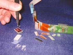
Another application of APDs is in positron-emission tomography (PET). A drug or metabolic probe can be labeled with a radioisotope that decays to produce a positron. The positron is annihilated by one of the electrons, producing two gamma rays almost 180° apart. Detection of the gamma rays localizes the source of the probe. This phenomenon can be used to study how a drug is metabolized, how it enters the brain, or how it affects blood flow or glucose utilization—useful both in clinical diagnostics and drug discovery. For drug discovery, it is necessary to at first study small animals such as rats, which requires a small PET scanner with many small detectors to localize the probe. A 32-channel APD array was designed just for this application (see photo at top of this page).


