
Peak-to-Valley (PV) and Root-Mean-Square (RMS) are two common parameters used to measure the difference between an ideal optic surface to the actual optic surface. Historically the PV is used more often than RMS but RMS is a much better method for measuring the feat of an optic. Neither one of them are perfect parameters to fully calculate the optics’ performance.
PV is the measurement of the height difference between the highest point and the lowest point on the surface of the optic. In an ideal world, the PV will solve the worst cases of the optics’ performance at the eyes of optics designer. This is only true if there is low order of aberration or large size features on the optics. It also assumes that the measurements are precise and optics surface is noise free.
In reality, the surface of an optic has imperfections that are within less than 1mm to aperture. The measurement is also processed with instrument having vast difference of MTF (modular transfer function) and noise level. Each manufacturer has its own proprietary “measuring method” to mask the actual measurements. It basically interpolates the standard parameters to something unknown to designers, professionals or vendors. This practice from manufacturers will be primarily based on the interpolator’s knowledge of optical performance and can quickly go out of control.
It is quite common to see cost and manufacturability to be determined purely upon the value of PV. Most will demand a 1/10 wave PV optics without specifying the testing condition and with minimum budget. This will result in an unworkable project or over priced component or reinterpreted specification by vendor. It is nearly impossible to get absolute 1/10 wave PV optics in the manufacturing process.
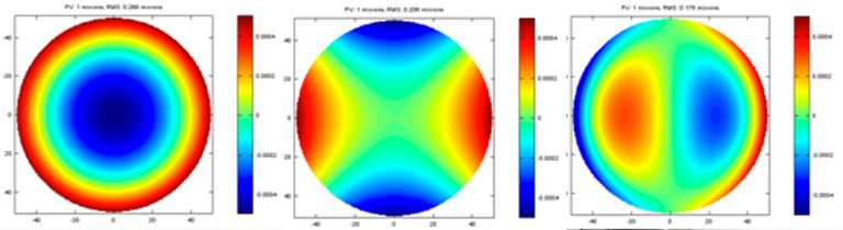
Plots of 1 micron PV for basic terms of aberration and its corresponding RMS are shown below. As you can see, the RMS is noticeably different for each basic term of aberration. Considering the similarity of alignment error in each system, the performance impact of each term is all relative to the ability of aligning specific error out at the final system.
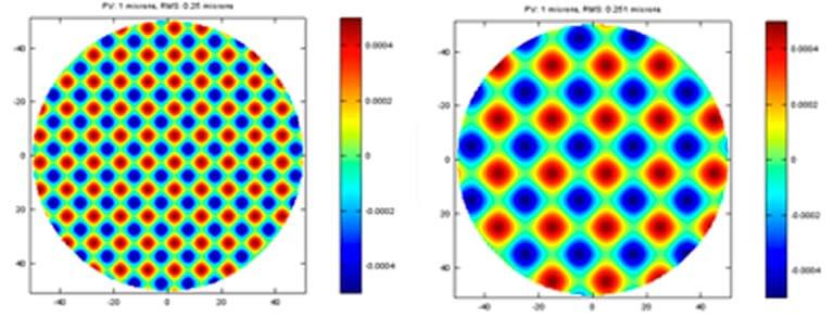
Modern optics is often made by sub-aperture polishing with computer controller motions. This creates another challenge when creating the specification of an optic. Due to the nature of sub-aperture polishing, the error on the surface is often showing as cyclical form. Two different frequency of this kind error is shown plots with the same 1-micron PV. If you can align most of the basic aberration in your system, this cyclical form error is not typically compensated in optical system. You notice that the PV and RMS are essential same or similar to the basic aberration terms, which is partially correctable at the system.
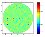
In well fabricated optics, the error mostly contains small but frequent imperfections plus occasional spikes of large but localized error. A simulated error of this kind is presented below. While the PV is still close to 1 microns, the RMS is much smaller than the errors shown previously. This is where the RMS really works while the PV completely fails to capture the quality of the optics.
The quality of optics should not be determined with just the numbers from PV or RMS. Contact Us for a free quote and consultation. With 20 years experience, we offer consulting service to help you find the specification you need for your optics.