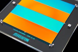
LAYERTEC, developer and manufacturer of high-quality laser components based in Mellingen, Thuringia, is currently expanding its range of customer-specific structuring of layer systems using lithography. Segmented components can be used for lateral phase and / or amplitude modulation and are therefore suitable for example for mode selection or beam splitting. The structured components are designed for use in high-power laser systems, the edges of the structures are laser-resistant up to the kW range.
Fused silica (plane) up to a size of currently 8 inches is used as the standard substrate material. On request, other materials are possible. Dielectric or metallic layers can be combined and applied in segments according to customer requirements. Depending on the layer design, structure sizes down to the µm range are possible as well as edge sharpness down to the single-digit µm range. The portfolio includes high-volume fabrication as well as flexible prototype manufacturing.
LAYERTEC was founded in 1990 as the first spin-off from the Friedrich Schiller University in Jena. Today, 30 years later, the company employs more than 300 people and operates worldwide. The company runs 40 coating chambers with different technologies and sizes for sputtering and evaporation. The in-house fine optics facility produces customer-specific plane, spherical, aspherical and free-form optics. Please do not hesitate to contact LAYERTEC for a quotation or a discussion regarding your special requirements.
Click here for more information.
