EV Group (EVG)

St Florian am Inn, UA 4782

COMPANY OVERVIEW

About EV Group (EVG)

850

Contact

DI Erich Thallner Str 1
St Florian am Inn, UA 4782
Austria
http://www.evgroup.com
43-771-253-110

More Info on EV Group (EVG)

EV Group (EVG) targets the global semiconductor, MEMS and nanotechnology markets with its industry-leading wafer-bonding, lithography/nanoimprint lithography (NIL), metrology, photoresist coating, cleaning and inspection equipment. www.EVGroup.com

Articles

Photo 241654721 © Marek Uliasz | Dreamstime.com
Dreamstime Xl 241654721
Executive Forum

Photonics business roundup: March 2022

Here, we recap all the photonics business news that was announced in March 2022.
FIGURE 1. The next generation of AR devices will display a FOV large enough to layer useful information over a significant expanse of natural human vision, while remaining lightweight and allowing the user to focus comfortably on both the information and the view.
Optics

Waveguides propel augmented reality to consumers

High-index glass wafers are the basis of flexible waveguide designs that bring a new generation of full-immersion augmented reality eyewear closer to fruition.
EVG
Optics

Schott, Inkron, EVG, and WaveOptics team up to fabricate next-gen waveguides for AR and MR devices

Introduced at SPIE's Photonics West 2020, the arrays of waveguide optics on high-index glass have wide field of view, aim for mass-production quantities.
EV Group
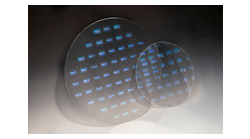
300 mm and 200 mm NIL wafers from EV Group
Optics

EVG & SCHOTT partner on 300 mm NIL wafers for AR/MR components

The work will take place at EVG’s NILPhotonics Competence Center, an open innovation incubator for nanoimprint lithography (NIL).
(Courtesy WaveOptics)
AR wearables such as smart glasses enable users to see digital images overlaid on top of the real world. WaveOptics' waveguide technology transfers light waves from the light source and projects them into the user's eye.
Optics

WaveOptics and EV Group collaborate on mass production of AR wearables

Goal is to produce low-cost, high-performance, waveguides for the consumer AR market.
(Image credit: SwissLitho)
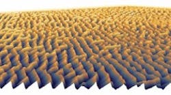
Topography image of a nanoimprint stamp of a 3D computer-generated hologram fabricated with the NanoFrazor from SwissLitho. Stamps such as these can be used to replicate 3D structures in high volume using the HERCULES NIL nanoimprint lithography system from EV Group.
Optics

EV Group and SwissLitho develop 3D nanoimprint lithography system with 1 nm accuracy

The joint solution enables the production of 3D semiconductor wafer structures down to the single-nanometer scale.
(Image credit: Fraunhofer ISE/A. Wekkeli)
A wafer-bonded III-V and silicon multi-junction solar cell with 30.2% efficiency beats theoretical limits.
Detectors & Imaging

Multi-junction solar cell exceeds theoretical limits at 30.2% efficiency

Fraunhofer ISE and EVG researchers developed a III-V/Si multi-junction solar cell that exceeds theoretical limits.
1401prod Evgroup
Optics

EV Group's automated UV nanoimprint litho system for photonics, LEDs and BioMEMS

The EVG 720 automated UV nanoimprint lithography system provides full-field lithography with an integrated soft stamp/template fabrication capability.

Buyer's Guide Listing Information

Click here for listing information and directions on how to add or update your company.

Request More Information From EV Group (EVG)

By clicking above, I acknowledge and agree to Endeavor Business Media’s Terms of Service and to Endeavor Business Media's use of my contact information to communicate with me about offerings by Endeavor, its brands, affiliates and/or third-party partners, consistent with Endeavor's Privacy Policy. In addition, I understand that my personal information will be shared with any sponsor(s) of the resource, so they can contact me directly about their products or services. Please refer to the privacy policies of such sponsor(s) for more details on how your information will be used by them. You may unsubscribe at any time.