KLA-Tencor

San Jose, CA 95134

COMPANY OVERVIEW

About KLA-Tencor

5600

Contact

160 Rio Pobles
MS D2129
San Jose, CA 95134
United States
http://www.kla-tencor.com
408-875-4460
408-875-4144

More Info on KLA-Tencor

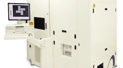
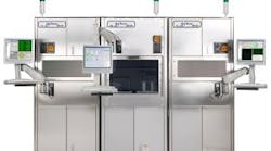
Provides optical surface analyzers that automatically detect and classify surface defects on optoelectronic and semiconductor wafers, including transparent wafers such as sapphire and glass.

Articles

(Credit: Gerd Altmann/Pixabay)
Digitization 4667378 1920
Home

Laser Focus World’s top 20 photonics technology picks for 2020

Photonics advances in 2020 include commercial hollow-core fiber, deep learning for numerous purposes, and advanced ultrafast lasers for materials processing.
FIGURE 1. The compact 3D interferometric optical profiler is shown (a) [4]; the x-y stage positions the sample and tilts in two directions to align the sample to the objective lens axis for interferometric measurement. The simplified optical layout (b) is also shown; the focal point of the objective lens is scanned vertically through the measurement distance. A low-coherence-length white-light LED is used for interferometric measurement of topography by WLI, PSI, and True Color measurement of the sample surface at each topographic height determined by interferometry.
Test & Measurement

3D optical interferometry with True Color visualization advances understanding of flexible electronics

Combining white-light interferometry (WLI), phase-shift interferometry (PSI), True Color imaging, and stitching into one optical profiler characterizes flexible electronics devices...
12 Lfw 12 Klatencor
Test & Measurement

KLA-Tencor metrology system extends overlay measurement capability

The Archer 500 overlay metrology system for logic and memory chip manufacturers enables lithographers to verify that pattern features have been correctly aligned.
Test & Measurement

Surfscan wafer inspection platform from KLA-Tencor first to use DUV illumination

Milpitas, CA--A new generation in KLA-Tencor's family of wafer inspection systems—the Surfscan SP3 with DUV illumination—was introduced for 28 nm and below semiconductor nodes...
Content Dam Etc Medialib Platform 7 Laser Focus World Articles Online Exclusive Articles 2010 Global 69214
Test & Measurement

Wafer inspection system allows defect inspection up to 200 mm

The ICOS WI-2250 wafer inspection system provides automated optical inspection for LED and MEMS products.
Optics

Cymer and KLA-Tencor announce collaboration at SPIE Microlithography

San Jose, CA--At the SPIE Microlithography meeting yesterday, Cymer (San Diego, CA) announced a collaboration with KLA-Tencor (San Jose, CA), in which Cymer will provide details...
Optics

Prolith lithography software optimizes design for manufacturability

San Jose, CA--In the last two decades, integrated-circuit (IC)-chip feature sizes have shrunk from a micron in width to one tenth that, and are still shrinking. Over that span...
FIGURE 1. A nine-element objective is corrected from 266 to 800 nm (top); it has an NA of 0.9, a field size of 0.13 mm, and is optimized to minimize the manufacturing tolerances and has reduced central obscuration. The objective has a standard object-to-flange distance of 45 mm. A seven-element objective is corrected from 266 to 800 nm (bottom); it has an NA of 0.9 and a field size of 0.13 mm.
Optics

Small catadioptric objectives extend microscopy into the deep-UV

Many microscopy applications can benefit from broadband deep-UV (DUV) imaging, some of which also require immersion, cover glass correction, or operation over a wide temperature...
Research

KLA-Tencor expands portfolio with Nanopro acquisition

KLA-Tencor (San Jose, CA) has acquired Nanopro (Frieburg, Germany), a privately held company specializing in advanced interferometric technology for measuring semiconductor-wafer...
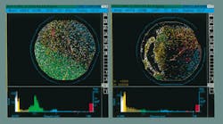
Polystyrene spheres, 0.496 mm in diameter, were deposited on the left half of a polished wafer and then scanned using circular polarization (left). The histogram at the bottom shows the detected size distribution of the spheres. The peak in the green area indicates that identical spheres are being detected as uniformly sized. The same wafer was scanned using linear polarization (right). Because linear polarization is unable to eliminate the effect of nonuniform film thickness, identical spheres in different locations have been detected as widely distributed in size. As a result, the green area of the histogram at the bottom has no peak.
Detectors & Imaging

How to correlate laser-scattering surface inspection

When mapping the surface of wafers, standard-diameter latex spheres can relate the scattering cross sections of different systems.

Buyer's Guide Listing Information

Click here for listing information and directions on how to add or update your company.

Request More Information From KLA-Tencor

By clicking above, I acknowledge and agree to Endeavor Business Media’s Terms of Service and to Endeavor Business Media's use of my contact information to communicate with me about offerings by Endeavor, its brands, affiliates and/or third-party partners, consistent with Endeavor's Privacy Policy. In addition, I understand that my personal information will be shared with any sponsor(s) of the resource, so they can contact me directly about their products or services. Please refer to the privacy policies of such sponsor(s) for more details on how your information will be used by them. You may unsubscribe at any time.