Pattern-transfer nanomanufacturing for micro-optics and spectroscopy

May 1, 2019
Programmable self-assembly of nanoparticle patterns enables a low-cost platform for nanoscale to mesoscale structures such as life-science substrates, custom diffraction gratings, and metasurfaces.

RYAN J. PRIORE

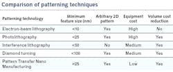
Patterned nanoscale structures hold tremendous promise for both the life-science and photonics industries. Such structures will enable substrates capable of capturing specific biological chemistries, optics to be directly integrated onto the tip of a fiber optic, and the next generation of polarizers and antireflective coatings using metasurfaces on flat or curved surfaces. To create 2D patterned structures at the nanoscale, companies presently use cleanroom microlithography originally developed for transistor manufacturing. Interference, photo-, and electron-beam lithography all have limitations when used for creating arbitrary 2D nanoscale structures in addition to more traditional optical fabrication tooling like diamond turning (see table).

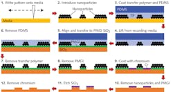
Electron-beam lithography is an expensive and low-throughput technique that can produce structures at the <100 nm scale. An electron beam is focused and rastered across a photosensitive coating atop of a substrate to create custom 2D patterns. Dry or wet etching is used to process the photosensitive coating into a final device or photomask for use with photolithography. In addition to its reliance upon a photomask generated by electron beam lithography, photolithography is not cost-effective for low-volume production. Interference lithography can produce dense optical features over a large area using coherent laser pulses, but is limited to uniformly distributed patterns such as those for creating dispersive gratings.An alternative approach created at CIRTEMO, called MagAssemble, is a nanomanufacturing process derived from hard-disk drive technology that takes advantage of the more than 50 years of research and development in that area to lower costs and increase manufacturing flexibility. Arbitrary 2D patterns (or templates) for organizing ferrous nanoparticles can be created by controlling the magnetic moments of cobalt-grain perpendicular magnetic recording media, which traditionally represent stored bits of data (see Fig. 1). These patterns may then be transferred to a variety of substrates for additional processing via dry and wet etching.1 This process, called Pattern Transfer Nano Manufacturing (PTNM), leads to capital costs for production that are on the order of 10% of those for lithography tooling. PTNM has a spatial resolution of better than 25 nm, which can be improved further based upon the selection of nanoparticles. The method consists of three key processing steps (see Fig. 2).

Step 1: Pattern write

A magnetic recording write/read head is brought into physical contact with perpendicular magnetic recording media. A high-resolution x-y translation stage moves the recording head back and forth across the recording media. Lubrication is used to reduce the friction between the recording head and the media. By switching the sign of the electric current injected into the recording head coil, a user-defined 2D template is created by controlling the magnetic transitions (that is, junctions between oppositely recorded regions) with high spatial resolution. The created template is stable for 10 years and can be erased/rerecorded if necessary.

Nanoparticle suspension solutions may be created by dispersing magnetic nanoparticles, which are uniform distributions with a magnetite (Fe3O4) particle diameter available from 10 to 30 nm, in solvents with appropriate concentrations. Custom-made magnetic nanoparticles such as magnetic core/gold shell particles may be used for applications requiring appropriate surface properties.

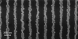
Once the 2D template is introduced into a magnetic nanoparticle suspension, the nanoparticles self-assemble along the magnetic transitions to create the final master pattern (see Fig. 3). The magnetic-field strength gradient at the transition can reach as high as 25 MT m-1 at 10 nm above the surface, resulting in nanoparticles firmly affixed to the substrate media.2 Functionalized magnetic particles may also be utilized at this point to create custom life-science substrates based directly on the recording media (as opposed to carrying out the additional steps 2 and 3) for either spatial isolation of a sample or purification.
Custom diffractive optical elements for spectroscopy and micro-optics are ideally suited to the PTNM process. CIRTEMO has developed a variety of product offerings including traditional dispersive gratings, mosaic arrays of gratings, and arbitrary 2D image transfers like zone plates or custom images (see Fig. 4).
REFERENCES

1. L. Ye et al., Adv. Funct. Mater., 26, 3983–3989 (2016).

2. L. Ye et al., Sci. Rep., 6, 23145, 1–9 (2016).

Ryan J. Priore is chief technology officer at CIRTEMO, Columbia, SC; e-mail: [email protected]; www.cirtemo.com. (Please note that as of May 1, 2019, CIRTEMO has joined the Thorlabs organization.)

Sponsored Recommendations

Request a quote: Micro 3D Printed Part or microArch micro-precision 3D printers

April 11, 2024
See the results for yourself! We'll print a benchmark part so that you can assess our quality. Just send us your file and we'll get to work.

Request a Micro 3D Printed Benchmark Part: Send us your file.

April 11, 2024
See the results for yourself! We'll print a benchmark part so that you can assess our quality. Just send us your file and we'll get to work.

Request a free Micro 3D Printed sample part

April 11, 2024
The best way to understand the part quality we can achieve is by seeing it first-hand. Request a free 3D printed high-precision sample part.

How to Tune Servo Systems: The Basics

April 10, 2024
Learn how to tune a servo system using frequency-based tools to meet system specifications by watching our webinar!

Voice your opinion!

To join the conversation, and become an exclusive member of Laser Focus World, create an account today!