SD-2 Silicon to Glass Bonding Wafers

May 5, 2014
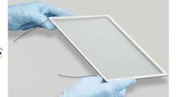
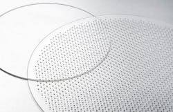
The SD-2 glass substrate has been designed with a coefficient thermal expansion curve that closely matches a Si single crystal. Silicon and glass wafers are typically put together via Anodic bonding. When this bonding is performed at 400 degree C, the differences of expansions at high temperatures can create residual stress in Si chips while they cool to room temperature. This is what can cause the distortion and bowing effects. HOYA’s SD-2 glass substrate matches CTE to Si wafers and has been optimized for Anodic bonding. This is especially useful in applications involving semiconductors, pressure sensors, displacement sensors, and photo-lithography.
By clicking above, I acknowledge and agree to Endeavor Business Media’s Terms of Service and to Endeavor Business Media's use of my contact information to communicate with me about offerings by Endeavor, its brands, affiliates and/or third-party partners, consistent with Endeavor's Privacy Policy. In addition, I understand that my personal information will be shared with any sponsor(s) of the resource, so they can contact me directly about their products or services. Please refer to the privacy policies of such sponsor(s) for more details on how your information will be used by them. You may unsubscribe at any time.