SCOTT SULLIVAN
Once the exclusive play toy of well-funded research labs, femtosecond lasers are starting to gain popularity for a range of industrial micromachining applications. Depending on the application or materials, micromachining tools incorporating femtosecond lasers give manufacturers a way to accommodate the ever-smaller and thinner components in consumer electronics, medical, and automotive markets, to name a few—and to do so profitably. Driving the trend is the fact that femtosecond lasers are getting smaller, growing more powerful, and covering more of the spectral range, while also coming down in price.
Ultrafast pulse lasers are generally defined as having a pulse length of <1ns. Femtosecond lasers take that much further, producing high-quality ultrafast pulses with a duration ranging from 30 to 800fs. How short is this in human terms? One way to look at it is to compare the time that the laser is on to the time that it is off. A typical usage model could be a 100fs laser pulse with a repetition rate of 100KHz. If 100fs were converted to 1s, the next pulse would occur in about 3.5 years! This effectively minimizes the time when heat can affect a material, and maximizes the amount of time when the material can thermally relax.
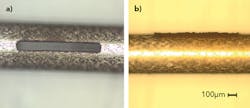
Femtosecond lasers offer a number of advantages over other types of lasers. A key advantage is that the heat-affected zone (HAZ) tends to be smaller than that of nanosecond or picosecond lasers (FIGURE 1). Ablation without thermal damage of the surrounding zones (known as cold ablation) is mandatory for the fabricating stents and is used to improve the strength and quality of automotive and consumer electronics. It also minimizes micro-crack formation when working with fragile or brittle materials, such as when processing hardened glass for smartphones, tablets, or wearable devices.
Another beneficial characteristic of femtosecond lasers stems from the high intensities (above 1012W/cm2) involved that literally break materials apart at an atomic level. Essentially, a microscopic plasma forms and material is removed during the resulting expansion. The low levels of debris are particularly beneficial for applications that involve drilling deeper holes with a high aspect ratio.
Ultra-thin and difficult material processing
Modern displays of all shapes and sizes use thin glass sheets, films, and foils to build up the display structure, including polarizers as well as a color filter, cover glass, and touch panel. Lasers provide a way to speed up processing and boost yield through repeatable, contact-free processing. They also enable new products that incorporate such features as ultra-thin glass, conformal cutting, or novel material combinations.
Ceramics such as aluminum nitride, aluminum oxide, silicon nitride, and zirconium oxide are high-performance materials gaining popularity for a wide variety of applications. They offer good electrical insulation properties and high temperature resistance and are becoming an integral in mobile phone antennas and high-performance light-emitting diode (LED) packages, to name a few.
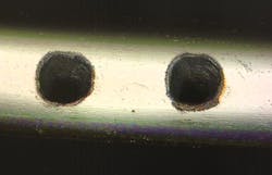
Drilling and cutting ceramics is an area where femtosecond lasers excel, enabling manufacturers to obtain high-quality geometries. The holes feature precise shapes, smooth inner walls, and minimal surface debris (FIGURE 2). Since very little to no post-processing is required, femtosecond lasers often provide significant yield gains and reduce manufacturing costs.For strengthened glass applications, femtosecond laser micromachining tools can easily achieve high-quality straight, curvilinear, and internal cuts that are extremely challenging for mechanical systems. High-peak-power femtosecond lasers can achieve high processing speeds with excellent edge quality and edge strength
Thin material removal
The increase in complexity and density of integrated circuits brings new manufacturing challenges to the semiconductor industry. For example, semiconductor wafers continue to see their thickness decrease, use multiple materials, and exhibit smaller feature sizes. Traditional manufacturing methods are reaching their limits.
The quality and accuracy of material processing enabled by ultrafast lasers make them a tool of choice for these new applications. In a selective ablation process example, it is possible to remove a thin layer of material—a few tens of nanometers thick—without affecting the underlying layer.
Minimal impact marking and engraving
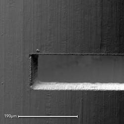
Product trademark recognition and traceability induced by standard and anti-counterfeiting solutions are essential for modern manufacturing methodologies. Internal laser marking of materials is an attractive solution for a variety of applications. However, in slower pulsed laser systems, the pulse duration of the marking laser is long enough to thermally generate micro-cracks in the material, which is detrimental to quality and long-term reliability. Femtosecond lasers concentrate the energy in such a short pulse duration that heat cannot be transferred to the surrounding material. The marking process then becomes effectively athermal, and micro-cracks cannot develop (FIGURE 3).Laser marking has a number of advantages compared to alternatives, including more consistent appearance, durability, and ease of application. Laser marking is visually appealing, primarily because the markings can have high-contrast color and uniform optical density. Laser marks can be generated that feature dark blacks and brilliant whites, depending on the type of process and material. Durability and visual quality is especially important for devices that will be handled extensively, such as smartphones and wearable devices. Femtosecond pulse lengths extend the application of laser marking by reducing surface impact, and can be used with thin materials.
Precise material removal of the surface of metals is a common technique used to create visual contrasting appearances for marking applications. Femtosecond lasers, because of their high peak power, can offer more efficient engraving rates of many materials, and can scale effectively to high power while preserving surface quality. The absence of thermal accumulation in the material can enable high-quality machining at a variety of depths and with a range of surface textures that can drive differentiation in a product's appearance.
Femtosecond laser tool solutions
Regardless of the application or laser pulse duration, successful micromachining with lasers involves precisely tailoring the laser pulse duration and power intensity to achieve the desired result. This requires a deep understanding of laser-material interaction to adjust variables such as pulse length, pulse energy, spot size, laser technology, and other factors. When these factors are properly tuned for the task at hand, femtosecond laser tools can be the tool of choice for many applications.
When making the move to femtosecond lasers, look for a tool supplier with deep laser-material knowledge and with the ability to support both short-run and high-volume applications. Many manufacturers make the mistake of assuming that all lasers are the same. The fact is that because of slight variations in optics, every laser will function somewhat differently from the next. Therefore, every tool in a manufacturing line should be accurately calibrated by the laser tool supplier to accommodate these variations and ensure consistent results.
Just as ultrafast lasers can lightly touch a surface, we have yet to fully discover and tap into all the possible applications for femtosecond lasers. One thing is clear, however: as systems and devices become smaller and more complex, femtosecond lasers will be increasingly involved in bringing them to market.
SCOTT SULLIVAN ([email protected]) is business development manager at Electro Scientific Industries (ESI), Portland, OR; www.esi.com.


