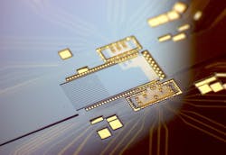
The field of photonic integrated circuits (PICs) has experienced remarkable growth in recent years, enabling a wide range of applications such as high-speed data communications, advanced sensing technologies, and LiDAR systems. But to fully unlock the potential of integrated photonics, efficient and innovative packaging solutions are essential.
Packaging covers a range of techniques and technical competencies to improve signal and power distribution, enhance optical performance, manage thermal effects, and provide mechanical, electrical, and environmental protection to the devices while at the same time enabling their connection to the outside world. It encompasses processes like die bonding, polishing, active alignment, hermetic sealing, and more.
PIXAPP and PHIX
European companies are now at the forefront of developing groundbreaking approaches to the packaging of PICs, also known as photonic chips. One notable reference point for PICs in Europe is PIXAPP, a distributed pilot line with partners across the continent.
PIXAPP has expanded its capacity and technological capabilities, particularly in prototype packaging development. It offers a comprehensive range of technologies, provides training, engages in high-risk development and early-stage prototyping, and grants companies access to cutting-edge equipment. PIXAPP establishes packaging standards based on design rules for optical and electrical packaging to facilitate customer configuration of devices. These design rules are expanding to encompass co-packaging optics with electronics, and even MEMS integration for applications like LiDAR and time of flight. While initially focused on early-stage prototyping, PIXAPP recognizes the need to develop the supply chain and packaging technology for scalable manufacturing.
PIXAPP’s packaging services and support span various application domains, including datacom, sensing, and medical sectors. They prioritize low-cost packaging, offering volume services to address the needs of high-end markets like datacom. Their pilot line has evolved to include advanced packaging technologies such as wafer-level packaging to enable cost reductions and increased packaging efficiency. Reliability is a key focus for PIXAPP, and comprehensive testing plays a vital role. Accelerated lifetime testing, including high-temperature storage, humidity, and mechanical stress testing, allows potential failure modes to be identified and addressed. PIXAPP is also actively developing standard reliability qualification protocols to ensure high levels of device robustness.
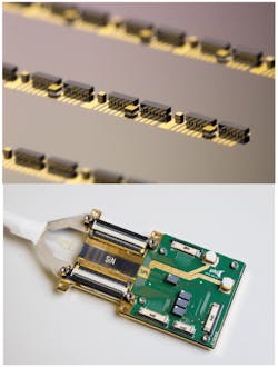
One of PIXAPP’s packaging partners is the Dutch company PHIX. For prototype packaging, PHIX offers flexible and easily adaptable standard packages that can be configured like Lego building blocks. These packages are available for various chip dimensions and electrical pad configurations, and for radio-frequency (RF) interfacing, modules can be upgraded with custom RF interfacing boards. In volume packaging, customers using standardized housings benefit from PHIX having them in stock, which eliminates the need for minimum order quantities or upfront housing design costs. This streamlined approach makes it easier for customers to prototype their customized products, qualify them for specific markets, or showcase them to investors and potential customers.
To scale up production, PHIX focuses on reducing the operator impact on production costs by implementing batch-level automation in their toolset—ensuring flexibility for scaling up production volumes. Once the volumes for a specific PIC reach a certain threshold, a dedicated production line can be established to further drive costs down and scale up.
PHIX remains attentive to market trends and needs, aiming to push the limits of hybrid integration by incorporating co-packaged optics, chipsets, and heterogeneous integration using different chip technologies such as indium phosphide, silicon nitride, and polyboards. They recognize the importance of miniaturization, but also emphasize increasing input/output (I/Os), functionality, area, and working with higher frequencies.
The efforts of organizations like PIXAPP and PHIX, supported by the collaborative spirit of EPIC, are driving the advancement of PIC packaging in Europe. These innovative approaches and technologies are crucial for enabling the widespread adoption of PICs across various industries, facilitating the development of cutting-edge applications, and pushing the boundaries of what’s possible in photonics. As the field continues to evolve, European companies are well positioned to lead the way in developing efficient, reliable, and cost-effective packaging solutions for the next generation of PICs.
ICON Photonics
ICON Photonics, based in France, specializes in polymer-based technology for chip-to-fiber interconnects. With a focus on densities, higher speeds, and wafer-level packaging, ICON Photonics offers a comprehensive solution by integrating photonics, electronics, and mechanics at the wafer level. This approach enables multiple solutions and ultra-low-loss coupling, catering to a diverse range of applications.
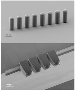
ICON Photonics provides mechanical fixtures for fiber array self-alignment and attachment, polymer tapered micro-optics for efficient light coupling, and the embedding of active devices such as detectors, edge-emitting-lasers (EELs), vertical-cavity surface-emitting lasers (VCSELs), as well as transition edge sensors and single-photon detectors for cryogenic quantum application. Their silicon interposers approach offers RF and millimeter-wave transmission lines, which further enhances their comprehensive packaging capabilities.
AT&S and Vario-optics
Other European players, AT&S and Vario-optics, place a strong emphasis on interconnecting photonic chips with a high number of electrical and optical interfaces for very cost-efficient photonic packages. They adopt a co-engineering approach that considers packaging requirements even before PIC fabrication begins. The multidisciplinary nature of PICs necessitates a collaborative effort.
Vario-optics’ packaging platform revolves around electro-optical circuit boards (EOCBs), which comprise planar waveguides with a high number of I/O channels and optical fanouts combined with electrical traces. These elements enable efficient electrical and optical coupling between the PIC and EOCB. The platform also includes optical interfaces to facilitate efficient PIC-waveguide coupling, along with the necessary electrical interfaces for metallization and integration with printed circuit boards. This comprehensive and cost-effective approach ensures optimal performance and seamless integration of PICs into the packaging process.
Nanoscribe, ficonTEC, and Yelo
As the demand for advanced photonic-enabled components, devices, and modules continues to rise, equipment manufacturers like Nanoscribe, ficonTEC, and Yelo are playing a crucial role in developing cutting-edge manufacturing and testing solutions. With their expertise and innovative approaches, these companies are helping drive the progress of the photonics industry.
Nanoscribe, a manufacturer of 3D microfabrication systems, developed the Quantum X align printer to print polymer microlenses. Its use of two-photon grayscale lithography 2GL, a technique that provides precise control over the position and size of the polymerization process, sets it apart. By leveraging a femtosecond near-infrared laser, Nanoscribe can achieve remarkable accuracy in the printing process. The system uses galvo mirrors for beam positioning and a microscope objective to focus the laser light into the sample volume—enabling 3D printing directly onto photonic chips at both the chip and wafer levels.
An integrated confocal module enables precise mapping of surfaces to align the micro-optics precisely to predefined markers. The intuitive software nanoPrintX gives instant visual feedback on the position and spatial alignment of all elements relative to each other and to predefined positions on substrates. These capabilities of nanoPrintX makes aligned 3D printing with Quantum X align easy and allow aligned 3D printing of micro-optics on fibers, fiber arrays, chip facets, over grating couplers, and many other use cases free-space micro-optical coupling applications for PICs. Nanoscribe’s collaborative approach with partners such as PHIX and Printoptix ensures seamless integration with advanced packaging solutions.
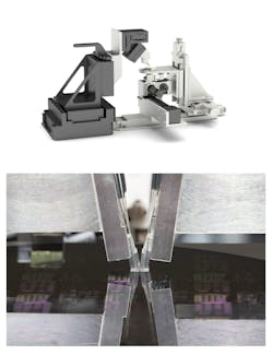
With a rich experience of over 20 years, ficonTEC manufactures configurable and modular advanced assembly and testing machines tailored for the production of photonic-enabled devices and systems for different market applications. They excel in two main functions: aligning and attaching micro-optics, optical fiber arrays, optoelectronic dies, and PICs using UV-cured epoxies, and thermal or laser-assisted eutectic bonding. Beyond this, ficonTEC offers comprehensive testing and qualifying capabilities, including validation and verification, electro-optical die and wafer-level testing, as well as electro-optical end-of-line testing. For bonding photonic chips, they developed a submicron accuracy alignment and assembly-IR system, which along with machine vision tools allows them to see through silicon PICs. This tool leverages the optical transparency of silicon beyond the infrared range, enabling passive alignment and direct coupling of active devices into waveguides and complex PIC structures by viewing from beneath the substrate or wafer.
ficonTEC also offers the “align-&-attach” platform, which combines high-precision optical alignment capabilities with various assembly technologies such as epoxy-based attachment, eutectic die bonding, and laser soldering. Its machine solutions can be configured and reconfigured to accommodate a wide range of research and process development, as well as batch and high-volume manufacturing tasks.
Testing is another critical stage in the development of photonic devices because it assesses their long-term reliability. This testing also serves as a parallel wafer qualification process to determine the optimal conditions for future burn-in, specifically the current and temperature at which the device will wear out. During life testing, Yelo carefully measures the optical degradation of laser diodes by monitoring changes in their operating characteristics. Determining the appropriate timing for burn-in presents a challenge. Performing burn-in too early, such as at the wafer level, may fail to detect certain failure modes. Conversely, delaying burn-in until after costly hermetic packaging can lead to high rejection costs. Typically, the optimal time for burn-in is after the chip has been separated, but before it is integrated into a more expensive package.
The field of PIC packaging is evolving rapidly, and these are a handful of a large number of European companies and research organizations that are at the forefront of developing innovative packaging solutions, as well as complementary solutions in 3D microfabrication, polymer-based circuit boards, and fiber coupling.
Standardized packaging, advanced materials, and testing techniques are driving the growth of photonics in various applications, including datacom, sensing, medical, and automotive. Optimized packaging processes, reduced costs, and improved reliability will pave the way for the widespread adoption of PICs in diverse industries, and a joint effort of all the players is required to achieve this in Europe.


